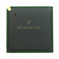
MPC562MZP56 Freescale Semiconductor, MPC562MZP56 Datasheet - Page 492

MPC562MZP56
Manufacturer Part Number
MPC562MZP56
Description
IC MPU 32BIT 56MHZ PPC 388-PBGA
Manufacturer
Freescale Semiconductor
Series
MPC5xxr
Datasheet
1.MPC561MZP56.pdf
(1420 pages)
Specifications of MPC562MZP56
Core Processor
PowerPC
Core Size
32-Bit
Speed
56MHz
Connectivity
CAN, EBI/EMI, SCI, SPI, UART/USART
Peripherals
POR, PWM, WDT
Number Of I /o
64
Program Memory Type
ROMless
Ram Size
32K x 8
Voltage - Supply (vcc/vdd)
2.5 V ~ 2.7 V
Data Converters
A/D 32x10b
Oscillator Type
External
Operating Temperature
-40°C ~ 125°C
Package / Case
388-BGA
Processor Series
MPC5xx
Core
PowerPC
Data Bus Width
32 bit
Data Ram Size
8 KB
Interface Type
SCI, SPI, UART
Maximum Clock Frequency
40 MHz
Number Of Programmable I/os
56
Number Of Timers
22
Operating Supply Voltage
2.6 V to 5 V
Maximum Operating Temperature
+ 85 C
Mounting Style
SMD/SMT
Minimum Operating Temperature
- 40 C
On-chip Adc
2 (10 bit, 32 Channel)
For Use With
MPC564EVB - KIT EVAL FOR MPC561/562/563/564
Lead Free Status / RoHS Status
Request inventory verification / Request inventory verification
Eeprom Size
-
Program Memory Size
-
Lead Free Status / Rohs Status
No
Available stocks
Company
Part Number
Manufacturer
Quantity
Price
Company:
Part Number:
MPC562MZP56
Manufacturer:
FREESCAL
Quantity:
204
Company:
Part Number:
MPC562MZP56
Manufacturer:
Freescale Semiconductor
Quantity:
10 000
Part Number:
MPC562MZP56
Manufacturer:
FREESCALE
Quantity:
20 000
Company:
Part Number:
MPC562MZP56R2
Manufacturer:
RFT
Quantity:
1 441
Company:
Part Number:
MPC562MZP56R2
Manufacturer:
Freescale Semiconductor
Quantity:
10 000
- Current page: 492 of 1420
- Download datasheet (11Mb)
QADC64E Legacy Mode Operation
operations have no effect. Each location in the CCW table corresponds to a location in the result word
table. When a conversion is completed for a CCW entry, the 10-bit result is written in the corresponding
result word entry. The QADC64E provides 64 CCW table entries.
The beginning of queue 1 is the first location in the CCW table. The first location of queue 2 is specified
by the beginning of queue 2 pointer (BQ2) in QACR2. To dedicate the entire CCW table to queue 1, queue
2 is programmed to be in the disabled mode, and BQ2 is programmed to 64 or greater. To dedicate the
entire CCW table to queue 2, queue 1 is programmed to be in the disabled mode, and BQ2 is specified as
the first location in the CCW
To prepare the QADC64E for a scan sequence, the software writes to the CCW table to specify the desired
channel conversions. The software also establishes the criteria for initiating the queue execution by
programming the queue operating mode. The queue operating mode determines what type of trigger event
causes queue execution to begin. A “trigger event” is used to refer to any of the ways to cause the
QADC64E to begin executing the CCWs in a queue or sub-queue. An “external trigger” is only one of the
possible “trigger events.”
13-28
0x27E (ccw63)
0x200 (ccw0)
P = Pause After Conversion
BYP = Bypass Buffer Amplifier
IST = Input Sample Time
CHAN = Channel Number
and End_of_Queue Code
Note 1: These offsets must be added to the module base address: A = 0x30 4800 or B = 0x30 4C00.
BQ2
P BYP IST
1
1
10-bit Conversion
Conversion Command
Command Word
Word (CCW) Table
(CCW) Format
Begin Queue 1
End of Queue 1
Begin Queue 2
End of Queue 2
Figure 13-15. QADC64E Conversion Queue Operation
table.Figure 13-15
CHAN
MPC561/MPC563 Reference Manual, Rev. 1.2
Analog to Digital
Channel Select,
Sample, Hold,
Conversion
A/D Converter
illustrates the operation of the queue structure.
and
Right Justified, Unsigned Result Format
0 0
0
S
Left Justified, Unsigned Result Format
0
0
Left Justified, Signed Result Format
0 0 0
in 3 Different 16-bit Formats
Result
Result
0
5 6
Software Readable
10-bit Result is
Result Word Table
Result
9 10
9 10
0 0
0 0
0 0 0
0
0 0
15
15
15
Freescale Semiconductor
0
0
Result 0
Result 63
Address Offsets
0x280-0x2FF
0x300-0x37F
S = Sign bit
0x380-0x3FF
1
1
1
Related parts for MPC562MZP56
Image
Part Number
Description
Manufacturer
Datasheet
Request
R
Part Number:
Description:
Mpc562 32 Bit Powerpc Microcontroller
Manufacturer:
Freescale Semiconductor, Inc
Datasheet:

Part Number:
Description:
MPC5 1K0 5%
Manufacturer:
TE Connectivity
Datasheet:

Part Number:
Description:
MPC5 500R 5%
Manufacturer:
TE Connectivity
Datasheet:

Part Number:
Description:
MPC5 5K0 5%
Manufacturer:
Tyco Electronics
Datasheet:

Part Number:
Description:
MPC5 5R0 5%
Manufacturer:
Tyco Electronics
Datasheet:

Part Number:
Description:
MPC5 50K 5%
Manufacturer:
Tyco Electronics
Datasheet:
Part Number:
Description:
Manufacturer:
Freescale Semiconductor, Inc
Datasheet:
Part Number:
Description:
Manufacturer:
Freescale Semiconductor, Inc
Datasheet:
Part Number:
Description:
Manufacturer:
Freescale Semiconductor, Inc
Datasheet:
Part Number:
Description:
Manufacturer:
Freescale Semiconductor, Inc
Datasheet:
Part Number:
Description:
Manufacturer:
Freescale Semiconductor, Inc
Datasheet:


