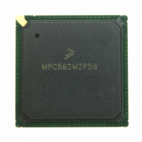
MPC562MZP56 Freescale Semiconductor, MPC562MZP56 Datasheet - Page 776

MPC562MZP56
Manufacturer Part Number
MPC562MZP56
Description
IC MPU 32BIT 56MHZ PPC 388-PBGA
Manufacturer
Freescale Semiconductor
Series
MPC5xxr
Datasheet
1.MPC561MZP56.pdf
(1420 pages)
Specifications of MPC562MZP56
Core Processor
PowerPC
Core Size
32-Bit
Speed
56MHz
Connectivity
CAN, EBI/EMI, SCI, SPI, UART/USART
Peripherals
POR, PWM, WDT
Number Of I /o
64
Program Memory Type
ROMless
Ram Size
32K x 8
Voltage - Supply (vcc/vdd)
2.5 V ~ 2.7 V
Data Converters
A/D 32x10b
Oscillator Type
External
Operating Temperature
-40°C ~ 125°C
Package / Case
388-BGA
Processor Series
MPC5xx
Core
PowerPC
Data Bus Width
32 bit
Data Ram Size
8 KB
Interface Type
SCI, SPI, UART
Maximum Clock Frequency
40 MHz
Number Of Programmable I/os
56
Number Of Timers
22
Operating Supply Voltage
2.6 V to 5 V
Maximum Operating Temperature
+ 85 C
Mounting Style
SMD/SMT
Minimum Operating Temperature
- 40 C
On-chip Adc
2 (10 bit, 32 Channel)
For Use With
MPC564EVB - KIT EVAL FOR MPC561/562/563/564
Lead Free Status / RoHS Status
Request inventory verification / Request inventory verification
Eeprom Size
-
Program Memory Size
-
Lead Free Status / Rohs Status
No
Available stocks
Company
Part Number
Manufacturer
Quantity
Price
Company:
Part Number:
MPC562MZP56
Manufacturer:
FREESCAL
Quantity:
204
Company:
Part Number:
MPC562MZP56
Manufacturer:
Freescale Semiconductor
Quantity:
10 000
Part Number:
MPC562MZP56
Manufacturer:
FREESCALE
Quantity:
20 000
Company:
Part Number:
MPC562MZP56R2
Manufacturer:
RFT
Quantity:
1 441
Company:
Part Number:
MPC562MZP56R2
Manufacturer:
Freescale Semiconductor
Quantity:
10 000
- Current page: 776 of 1420
- Download datasheet (11Mb)
Modular Input/Output Subsystem (MIOS14)
17-44
SRESET
Bits
0
1
2
3
4
5
Field PIN WOR FREN
Addr
FORCA
EDPOL
MSB
Name
FREN
WOR
—
0
PIN
—
0x30 605E, 0x30 6066, 0x30 606E, 0x30 6076, 0x30 607E, 0x30 60DE, 0x30 60E6, 0x30 60EE,
1
Pin Input Status — The pin input status bit reflects the status of the corresponding bit.
Wired-OR bit — In the DIS, IPWM, IPM and IC modes, the WOR bit is not used; reading this bit
returns the value that was previously written.
In the OCB, OCAB and OPWM modes, the WOR bit selects whether the output buffer is
configured for open-drain or totem pole operation. When open-drain mode is selected, the
EDPOL bit is not used; writing to EDPOL will have no effect on the output voltage.
1 Output buffer is open-drain.
0 Output buffer is totem pole.
The WOR bit is cleared by reset.
Freeze enable bit — This active high read/write control bit enables the MDASM to recognize the
MIOB freeze signal.
1 = The MDASM is frozen if the MIOB freeze line is active.
0 = The MDASM is not frozen even if the MIOB freeze line is active.
The FREN is cleared by reset.
Reserved
Polarity bit — In the DIS mode, this bit is not used; reading it returns the last value written.
In the IPWM mode, this bit is used to select the capture edge sensitivity of channels A and B.
1 Channel A captures on a falling edge. Channel B captures on a rising edge.
0 Channel A captures on a rising edge. Channel B captures on a falling edge.
In the IPM and IC modes, the EDPOL bit is used to select the input capture edge sensitivity of
channel A.
1 Channel A captures on a falling edge.
0 Channel A captures on a rising edge.
In the OCB, OCAB and OPWM modes, the EDPOL bit is used to select the voltage level on the
output signal. If open-drain mode is selected via the WOR bit, the EDPOL bit is disabled and
writing to it will have no effect on the output voltage.
1 The complement of the output flip-flop logic level appears on the output signal: a match on
0 The output flip-flop logic level appears on the output signal: a match on channel A sets the
The EDPOL bit is cleared by reset.
Force A bit — In the OCB, OCAB and OPWM modes, the FORCA bit allows the software to force
the output flip-flop to behave as if a successful comparison had occurred on channel A (except
that the FLAG line is not activated). Writing a one to FORCA sets the output flip-flop; writing a
zero to it has no effect.
In the DIS, IPWM, IPM and IC modes, the FORCA bit is not used and writing to it has no effect.
FORCA is cleared by reset and is always read as zero.
Writing a one to both FORCA and FORCB simultaneously resets the output flip-flop.
Figure 17-24. MDASM Status/Control Register (MDASMSCR)
channel A resets the output signal; a match on channel B sets the output signal.
output signal, a match on channel B resets the output signal.
2
—
Table 17-21. MDASMSCR Bit Descriptions
3
MPC561/MPC563 Reference Manual, Rev. 1.2
EDPOL FORCA FORCB
4
5
0x30 60F6, 0x30 60FE
000_0000_0000_0000
6
Description
7
—
8
9
BSL
10
—
11
Freescale Semiconductor
12
13
MODE
14
LSB
15
Related parts for MPC562MZP56
Image
Part Number
Description
Manufacturer
Datasheet
Request
R
Part Number:
Description:
Mpc562 32 Bit Powerpc Microcontroller
Manufacturer:
Freescale Semiconductor, Inc
Datasheet:

Part Number:
Description:
MPC5 1K0 5%
Manufacturer:
TE Connectivity
Datasheet:

Part Number:
Description:
MPC5 500R 5%
Manufacturer:
TE Connectivity
Datasheet:

Part Number:
Description:
MPC5 5K0 5%
Manufacturer:
Tyco Electronics
Datasheet:

Part Number:
Description:
MPC5 5R0 5%
Manufacturer:
Tyco Electronics
Datasheet:

Part Number:
Description:
MPC5 50K 5%
Manufacturer:
Tyco Electronics
Datasheet:
Part Number:
Description:
Manufacturer:
Freescale Semiconductor, Inc
Datasheet:
Part Number:
Description:
Manufacturer:
Freescale Semiconductor, Inc
Datasheet:
Part Number:
Description:
Manufacturer:
Freescale Semiconductor, Inc
Datasheet:
Part Number:
Description:
Manufacturer:
Freescale Semiconductor, Inc
Datasheet:
Part Number:
Description:
Manufacturer:
Freescale Semiconductor, Inc
Datasheet:


