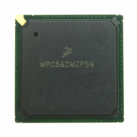
MPC562MZP56 Freescale Semiconductor, MPC562MZP56 Datasheet - Page 879

MPC562MZP56
Manufacturer Part Number
MPC562MZP56
Description
IC MPU 32BIT 56MHZ PPC 388-PBGA
Manufacturer
Freescale Semiconductor
Series
MPC5xxr
Datasheet
1.MPC561MZP56.pdf
(1420 pages)
Specifications of MPC562MZP56
Core Processor
PowerPC
Core Size
32-Bit
Speed
56MHz
Connectivity
CAN, EBI/EMI, SCI, SPI, UART/USART
Peripherals
POR, PWM, WDT
Number Of I /o
64
Program Memory Type
ROMless
Ram Size
32K x 8
Voltage - Supply (vcc/vdd)
2.5 V ~ 2.7 V
Data Converters
A/D 32x10b
Oscillator Type
External
Operating Temperature
-40°C ~ 125°C
Package / Case
388-BGA
Processor Series
MPC5xx
Core
PowerPC
Data Bus Width
32 bit
Data Ram Size
8 KB
Interface Type
SCI, SPI, UART
Maximum Clock Frequency
40 MHz
Number Of Programmable I/os
56
Number Of Timers
22
Operating Supply Voltage
2.6 V to 5 V
Maximum Operating Temperature
+ 85 C
Mounting Style
SMD/SMT
Minimum Operating Temperature
- 40 C
On-chip Adc
2 (10 bit, 32 Channel)
For Use With
MPC564EVB - KIT EVAL FOR MPC561/562/563/564
Lead Free Status / RoHS Status
Request inventory verification / Request inventory verification
Eeprom Size
-
Program Memory Size
-
Lead Free Status / Rohs Status
No
Available stocks
Company
Part Number
Manufacturer
Quantity
Price
Company:
Part Number:
MPC562MZP56
Manufacturer:
FREESCAL
Quantity:
204
Company:
Part Number:
MPC562MZP56
Manufacturer:
Freescale Semiconductor
Quantity:
10 000
Part Number:
MPC562MZP56
Manufacturer:
FREESCALE
Quantity:
20 000
Company:
Part Number:
MPC562MZP56R2
Manufacturer:
RFT
Quantity:
1 441
Company:
Part Number:
MPC562MZP56R2
Manufacturer:
Freescale Semiconductor
Quantity:
10 000
- Current page: 879 of 1420
- Download datasheet (11Mb)
Freescale Semiconductor
13:14
9:10
Bits
4:5
6:8
11
12
15
0
1
2
3
DBGC[0:1]
Name
EARB
BDRV
ATWC
EBDF
BDIS
BPS
IWS
—
—
IP
External arbitration — Refer to
arbitration. The default value is that internal arbitration hardware is used.
0 Internal arbitration is performed
1 External arbitration is assumed
Initial interrupt prefix — This bit defines the initial value of the MSR[IP] immediately after reset. The
MSR[IP] bit defines the Interrupt Table location.
0 MSR[IP] = 0 after reset
1 MSR[IP] = 1 after reset
The default value is 0. See
Bus pins drive strength — This bit determines the bus pins’ (address, data, and control) driving
capability to be either full or reduced drive. The bus default drive strength is full; upon default, it also
causes the CLKOUT drive strength to be full. See
default state of COM[1] in the SIUMCR.
0 Full drive
1 Reduced drive
Boot disable — If the BDIS bit is set, then memory controller is not activated after reset. If it is cleared
then the memory controller bank 0 is active immediately after reset such that it matches any addresses.
If a write to the OR0 register occurs after reset this bit definition is ignored. The default value is that the
memory controller is enabled to control the boot with the CS0 pin. See
Chip-Select
0 Memory controller bank 0 is active and matches all addresses immediately after reset
1 Memory controller is not activated after reset.
Boot port size — This field defines the port size of the boot device on reset (BR0[PS]). If a write to the
OR0 register occurs after reset this field definition is ignored. See
information.
00 32-bit port (default)
01 8-bit port
10 16-bit port
11 Reserved
Reserved. These bits must not be high in the reset configuration word.
Debug pins configuration — See
this field definition. The default value is that these pins function as: VFLS[0:1], BI, BR, BG and BB. See
Table
Reserved.
Address type write enable configuration — The default value is that these pins function as WE pins.
0 WE[0:3]/BE[0:3]/AT[0:3] functions as WE[0:3]/BE[0:3]
1 WE[0:3]/BE[0:3]/AT[0:3] functions as AT[0:3]
See
External bus division factor — This field defines the initial value of the external bus frequency. The
default value is that CLKOUT frequency is equal to that of the internal clock (no division). See
Interlock write select — This bit determines which interlock write operation should be used during the
clear censorship operation.
IWS always comes from the UC3FCFIG, it will never use the external reset configuration word
(RSTCONF=0) or the default internal reset configuration word (RSTCONF=1 and HC=1).
0 Interlock write is a write to any UC3F array location
1 Interlock write is a write to the UC3FMCR register.
Table
6-8.
6-7.
Operation” for more information.
MPC561/MPC563 Reference Manual, Rev. 1.2
Table 21-6. RCW Bit Descriptions
Table 3-11
Section 9.5.7, “Arbitration
Section 6.2.2.1.1, “SIU Module Configuration Register
for more information.
Description
Table 6-7
Phase” for a detailed description of Bus
for more information. BDRV controls the
Table 10-5
Section 10.7, “Global (Boot)
CDR3 Flash (UC3F) EEPROM
and
Table 10-8
(SIUMCR)” for
Table
for more
21-17
8-9.
Related parts for MPC562MZP56
Image
Part Number
Description
Manufacturer
Datasheet
Request
R
Part Number:
Description:
Mpc562 32 Bit Powerpc Microcontroller
Manufacturer:
Freescale Semiconductor, Inc
Datasheet:

Part Number:
Description:
MPC5 1K0 5%
Manufacturer:
TE Connectivity
Datasheet:

Part Number:
Description:
MPC5 500R 5%
Manufacturer:
TE Connectivity
Datasheet:

Part Number:
Description:
MPC5 5K0 5%
Manufacturer:
Tyco Electronics
Datasheet:

Part Number:
Description:
MPC5 5R0 5%
Manufacturer:
Tyco Electronics
Datasheet:

Part Number:
Description:
MPC5 50K 5%
Manufacturer:
Tyco Electronics
Datasheet:
Part Number:
Description:
Manufacturer:
Freescale Semiconductor, Inc
Datasheet:
Part Number:
Description:
Manufacturer:
Freescale Semiconductor, Inc
Datasheet:
Part Number:
Description:
Manufacturer:
Freescale Semiconductor, Inc
Datasheet:
Part Number:
Description:
Manufacturer:
Freescale Semiconductor, Inc
Datasheet:
Part Number:
Description:
Manufacturer:
Freescale Semiconductor, Inc
Datasheet:


