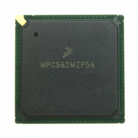
MPC562MZP56 Freescale Semiconductor, MPC562MZP56 Datasheet - Page 887

MPC562MZP56
Manufacturer Part Number
MPC562MZP56
Description
IC MPU 32BIT 56MHZ PPC 388-PBGA
Manufacturer
Freescale Semiconductor
Series
MPC5xxr
Datasheet
1.MPC561MZP56.pdf
(1420 pages)
Specifications of MPC562MZP56
Core Processor
PowerPC
Core Size
32-Bit
Speed
56MHz
Connectivity
CAN, EBI/EMI, SCI, SPI, UART/USART
Peripherals
POR, PWM, WDT
Number Of I /o
64
Program Memory Type
ROMless
Ram Size
32K x 8
Voltage - Supply (vcc/vdd)
2.5 V ~ 2.7 V
Data Converters
A/D 32x10b
Oscillator Type
External
Operating Temperature
-40°C ~ 125°C
Package / Case
388-BGA
Processor Series
MPC5xx
Core
PowerPC
Data Bus Width
32 bit
Data Ram Size
8 KB
Interface Type
SCI, SPI, UART
Maximum Clock Frequency
40 MHz
Number Of Programmable I/os
56
Number Of Timers
22
Operating Supply Voltage
2.6 V to 5 V
Maximum Operating Temperature
+ 85 C
Mounting Style
SMD/SMT
Minimum Operating Temperature
- 40 C
On-chip Adc
2 (10 bit, 32 Channel)
For Use With
MPC564EVB - KIT EVAL FOR MPC561/562/563/564
Lead Free Status / RoHS Status
Request inventory verification / Request inventory verification
Eeprom Size
-
Program Memory Size
-
Lead Free Status / Rohs Status
No
Available stocks
Company
Part Number
Manufacturer
Quantity
Price
Company:
Part Number:
MPC562MZP56
Manufacturer:
FREESCAL
Quantity:
204
Company:
Part Number:
MPC562MZP56
Manufacturer:
Freescale Semiconductor
Quantity:
10 000
Part Number:
MPC562MZP56
Manufacturer:
FREESCALE
Quantity:
20 000
Company:
Part Number:
MPC562MZP56R2
Manufacturer:
RFT
Quantity:
1 441
Company:
Part Number:
MPC562MZP56R2
Manufacturer:
Freescale Semiconductor
Quantity:
10 000
- Current page: 887 of 1420
- Download datasheet (11Mb)
lowest numbered block and will also be located in small block 0 if the lowest numbered block hosts a small
block in the implemented configuration.
21.3.7.3
The program operation may be suspended to allow read accesses to the array. Setting the HSUS bit in the
UC3FCTL to a 1 while PE = 0, EHV = 1, and HVS = 1 forces the array into a program suspend state. The
deassertion of the HVS bit (HVS = 0) signifies that the program operation has been successfully
suspended. The HVS bit should negate within 10µs of asserting the HSUS bit.
While in program suspend mode, normal read accesses may be performed to the UC3F array or shadow
information words. Reads to the array location targeted for program return indeterminate data since only
a partial programming operation may have been performed.
The program operation may be resumed by setting HSUS = 0.
21.3.8
To modify the charge stored in an isolated element of the UC3F bit from a logic 0 state to a logic 1 state,
an erase operation is required. In the UC3F EEPROM, erase is a bulk operatBlockion that affects the stored
charge of all the isolated elements in an array block. To make the UC3F module block-erasable, the array
is divided into blocks that are physically isolated from each other. Each of the array blocks may be erased
in isolation or in any combination. The UC3F array block size is fixed for all blocks in the module at 64
Kbytes and the module is comprised of eight blocks. Two of these blocks may be further subdivided into
two small blocks. Array blocks of the UC3F EEPROM that are protected (PROTECT[M] = 1 or
(SBEN[M] = 1 & SBPROTECT[M] = 1)) will not be erased. Also, if EPEE = 0 or B0EPEE = 0, no erase
voltages will be applied to the array or the block corresponding to block 0 or small block 0 if SBEN[0] = 1.
The embedded program/erase algorithm first pre-programs all bits in blocks selected for erase prior to
actually erasing the selected blocks.
The array blocks selected for erase operation are determined by BLOCK[0:7], SBBLOCK[0:1] in
conjunction with SBEN[0:1], and the array configuration. If multiple blocks are selected for erase, the
embedded erase hardware algorithm serially erases each array block until all of the selected blocks are
erased. For instance, if BLOCK[0:7] = 0x78 and SBEN[0:1] = 0b00, then blocks 1, 2, 3, and 4 are selected
for erase. The embedded erase hardware algorithm first erases block 1 and then erases block 2 followed
Freescale Semiconductor
Erasing
Program Suspend
Repeated suspending of a program operation to fetch array contents may
extend the program operation. The internal program hardware may only
resume the program operation at predefined steps of the internal program
hardware sequence; interrupting the program operation on a high frequency
basis may cause the internal program hardware to delay completion of the
current step and delay advancement to the next step of the internal program
hardware sequence. Frequent suspend/resume operations (more than
approximately once per millisecond) may also cause program or erase
timeouts, and are not recommended.
MPC561/MPC563 Reference Manual, Rev. 1.2
NOTE
CDR3 Flash (UC3F) EEPROM
21-25
Related parts for MPC562MZP56
Image
Part Number
Description
Manufacturer
Datasheet
Request
R
Part Number:
Description:
Mpc562 32 Bit Powerpc Microcontroller
Manufacturer:
Freescale Semiconductor, Inc
Datasheet:

Part Number:
Description:
MPC5 1K0 5%
Manufacturer:
TE Connectivity
Datasheet:

Part Number:
Description:
MPC5 500R 5%
Manufacturer:
TE Connectivity
Datasheet:

Part Number:
Description:
MPC5 5K0 5%
Manufacturer:
Tyco Electronics
Datasheet:

Part Number:
Description:
MPC5 5R0 5%
Manufacturer:
Tyco Electronics
Datasheet:

Part Number:
Description:
MPC5 50K 5%
Manufacturer:
Tyco Electronics
Datasheet:
Part Number:
Description:
Manufacturer:
Freescale Semiconductor, Inc
Datasheet:
Part Number:
Description:
Manufacturer:
Freescale Semiconductor, Inc
Datasheet:
Part Number:
Description:
Manufacturer:
Freescale Semiconductor, Inc
Datasheet:
Part Number:
Description:
Manufacturer:
Freescale Semiconductor, Inc
Datasheet:
Part Number:
Description:
Manufacturer:
Freescale Semiconductor, Inc
Datasheet:


