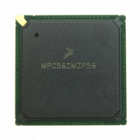
MPC562MZP56 Freescale Semiconductor, MPC562MZP56 Datasheet - Page 888

MPC562MZP56
Manufacturer Part Number
MPC562MZP56
Description
IC MPU 32BIT 56MHZ PPC 388-PBGA
Manufacturer
Freescale Semiconductor
Series
MPC5xxr
Datasheet
1.MPC561MZP56.pdf
(1420 pages)
Specifications of MPC562MZP56
Core Processor
PowerPC
Core Size
32-Bit
Speed
56MHz
Connectivity
CAN, EBI/EMI, SCI, SPI, UART/USART
Peripherals
POR, PWM, WDT
Number Of I /o
64
Program Memory Type
ROMless
Ram Size
32K x 8
Voltage - Supply (vcc/vdd)
2.5 V ~ 2.7 V
Data Converters
A/D 32x10b
Oscillator Type
External
Operating Temperature
-40°C ~ 125°C
Package / Case
388-BGA
Processor Series
MPC5xx
Core
PowerPC
Data Bus Width
32 bit
Data Ram Size
8 KB
Interface Type
SCI, SPI, UART
Maximum Clock Frequency
40 MHz
Number Of Programmable I/os
56
Number Of Timers
22
Operating Supply Voltage
2.6 V to 5 V
Maximum Operating Temperature
+ 85 C
Mounting Style
SMD/SMT
Minimum Operating Temperature
- 40 C
On-chip Adc
2 (10 bit, 32 Channel)
For Use With
MPC564EVB - KIT EVAL FOR MPC561/562/563/564
Lead Free Status / RoHS Status
Request inventory verification / Request inventory verification
Eeprom Size
-
Program Memory Size
-
Lead Free Status / Rohs Status
No
Available stocks
Company
Part Number
Manufacturer
Quantity
Price
Company:
Part Number:
MPC562MZP56
Manufacturer:
FREESCAL
Quantity:
204
Company:
Part Number:
MPC562MZP56
Manufacturer:
Freescale Semiconductor
Quantity:
10 000
Part Number:
MPC562MZP56
Manufacturer:
FREESCALE
Quantity:
20 000
Company:
Part Number:
MPC562MZP56R2
Manufacturer:
RFT
Quantity:
1 441
Company:
Part Number:
MPC562MZP56R2
Manufacturer:
Freescale Semiconductor
Quantity:
10 000
- Current page: 888 of 1420
- Download datasheet (11Mb)
CDR3 Flash (UC3F) EEPROM
by blocks 3 and 4. The total erase time for this example is the block erase time, T
since four blocks are erased. In addition, the preprogramming time to program all locations in blocks 1, 2,
3, and 4 to a “0” state needs to be considered when determining the total erase time. The preprogramming
time is dependent on the data already stored in the Flash array before beginning the erase operation.
21.3.8.1
The UC3F EEPROM module requires a sequence of writes to the high voltage control register
(UC3FCTL) and an erase interlock write in order to enable high voltage to the array and shadow
information for erase operation. The required hardware algorithm erase sequence follows.
21-26
1. Write PROTECT[0:7] and SBPROTECT[0:1] to disable protect for the blocks to be erased.
2. Write BLOCK[0:7] and SBBLOCK[0:1] to select the blocks to be erased, PE = 1 and SES = 1 in
3. Execute an erase interlock write to any UC3F array location.
4. Write EHV = 1 in the UC3FCTL register.
5. Read the UC3FCTL register until HVS = 0.
6. Read the UC3FCTL register. Confirm PEGOOD =1.
7. Write EHV = 0 in the UC3FCTL register.
8. Write SES =0 in the UC3FCTL register.
the UC3FCTL register.
Erase Sequence
BLOCK[0:7] and SBBLOCK[0:1] in conjunction with SBEN[0:1]
determine which blocks are selected for erase. Blocks whose BLOCK bits
or enabled small blocks whose SBBLOCK bits are set (equal to 1) get erased
when an erase operation is performed.
The values of the EPEE and B0EPEE inputs are latched with the assertion
of EHV to determine the array protection state for the erase operation. It is
assumed that the EPEE and B0EPEE inputs are setup prior to the assertion
of EHV.
Writing EHV = 0 before HVS = 0 causes the current erase sequence to
ABORT. All blocks being erased must go through another erase sequence
before the UC3F EEPROM can be used reliably.
MPC561/MPC563 Reference Manual, Rev. 1.2
WARNING
NOTE
NOTE
ERASE
Freescale Semiconductor
, multiplied by four
Related parts for MPC562MZP56
Image
Part Number
Description
Manufacturer
Datasheet
Request
R
Part Number:
Description:
Mpc562 32 Bit Powerpc Microcontroller
Manufacturer:
Freescale Semiconductor, Inc
Datasheet:

Part Number:
Description:
MPC5 1K0 5%
Manufacturer:
TE Connectivity
Datasheet:

Part Number:
Description:
MPC5 500R 5%
Manufacturer:
TE Connectivity
Datasheet:

Part Number:
Description:
MPC5 5K0 5%
Manufacturer:
Tyco Electronics
Datasheet:

Part Number:
Description:
MPC5 5R0 5%
Manufacturer:
Tyco Electronics
Datasheet:

Part Number:
Description:
MPC5 50K 5%
Manufacturer:
Tyco Electronics
Datasheet:
Part Number:
Description:
Manufacturer:
Freescale Semiconductor, Inc
Datasheet:
Part Number:
Description:
Manufacturer:
Freescale Semiconductor, Inc
Datasheet:
Part Number:
Description:
Manufacturer:
Freescale Semiconductor, Inc
Datasheet:
Part Number:
Description:
Manufacturer:
Freescale Semiconductor, Inc
Datasheet:
Part Number:
Description:
Manufacturer:
Freescale Semiconductor, Inc
Datasheet:


