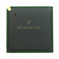
MPC562MZP56 Freescale Semiconductor, MPC562MZP56 Datasheet - Page 970

MPC562MZP56
Manufacturer Part Number
MPC562MZP56
Description
IC MPU 32BIT 56MHZ PPC 388-PBGA
Manufacturer
Freescale Semiconductor
Series
MPC5xxr
Datasheet
1.MPC561MZP56.pdf
(1420 pages)
Specifications of MPC562MZP56
Core Processor
PowerPC
Core Size
32-Bit
Speed
56MHz
Connectivity
CAN, EBI/EMI, SCI, SPI, UART/USART
Peripherals
POR, PWM, WDT
Number Of I /o
64
Program Memory Type
ROMless
Ram Size
32K x 8
Voltage - Supply (vcc/vdd)
2.5 V ~ 2.7 V
Data Converters
A/D 32x10b
Oscillator Type
External
Operating Temperature
-40°C ~ 125°C
Package / Case
388-BGA
Processor Series
MPC5xx
Core
PowerPC
Data Bus Width
32 bit
Data Ram Size
8 KB
Interface Type
SCI, SPI, UART
Maximum Clock Frequency
40 MHz
Number Of Programmable I/os
56
Number Of Timers
22
Operating Supply Voltage
2.6 V to 5 V
Maximum Operating Temperature
+ 85 C
Mounting Style
SMD/SMT
Minimum Operating Temperature
- 40 C
On-chip Adc
2 (10 bit, 32 Channel)
For Use With
MPC564EVB - KIT EVAL FOR MPC561/562/563/564
Lead Free Status / RoHS Status
Request inventory verification / Request inventory verification
Eeprom Size
-
Program Memory Size
-
Lead Free Status / Rohs Status
No
Available stocks
Company
Part Number
Manufacturer
Quantity
Price
Company:
Part Number:
MPC562MZP56
Manufacturer:
FREESCAL
Quantity:
204
Company:
Part Number:
MPC562MZP56
Manufacturer:
Freescale Semiconductor
Quantity:
10 000
Part Number:
MPC562MZP56
Manufacturer:
FREESCALE
Quantity:
20 000
Company:
Part Number:
MPC562MZP56R2
Manufacturer:
RFT
Quantity:
1 441
Company:
Part Number:
MPC562MZP56R2
Manufacturer:
Freescale Semiconductor
Quantity:
10 000
- Current page: 970 of 1420
- Download datasheet (11Mb)
READI Module
24.1.1
The functional block diagram of the READI module is shown in
24-2
•
•
•
•
•
•
•
•
Run-time access to on-chip memory map and MPC500 special purpose registers (SPRs) via the
READI read/write access protocol. This feature supports accesses for runtime internal visibility,
calibration constant acquisition and tuning, and external rapid prototyping for powertrain
automotive development systems.
Watchpoint messaging via the auxiliary port
Nine or 16 full-duplex auxiliary signal interface for medium and high visibility throughput
— One of two modes selected during reset: full port mode (FPM) and reduced port mode (RPM).
— Auxiliary output port
— Auxiliary input port
All features configurable and controllable via the auxiliary port
Security features for production environment
Support of existing RCPU development access protocol via the auxiliary port
READI module can be reset independent of system reset
Parametrics:
— Two bits are downloaded per clock in full port mode. For example, with input clock running at
— One bit is downloaded per clock in reduced port mode. For example, with input clock running
— Eight bits are uploaded per clock in full port mode. For example, with system clock running at
— Two bits are uploaded per clock in reduced port mode. For example, with system clock running
– FPM comprises 16 signals and RPM comprises nine signals
– One MCKO (message clock out) signal
– Two or eight MDO (message data out) signals
– One MSEO (message start/end out) signal
– One MCKI (message clock in) signal
– One or two MDI (message data in) signals
– One MSEI (message start/end in) signal
– One EVTI (event in) signal
– One RSTI (reset in) signal
28 MHz, this translates to a download rate of 56 Mbits/s.
at 28 MHz, this translates to a download rate of 28 Mbits/s.
56 MHz, this translates to a upload rate of 448 Mbits/s.
at 56 MHz, this translates to a upload rate of 112 Mbits/s.
Functional Block Diagram
MPC561/MPC563 Reference Manual, Rev. 1.2
Figure
24-1.
Freescale Semiconductor
Related parts for MPC562MZP56
Image
Part Number
Description
Manufacturer
Datasheet
Request
R
Part Number:
Description:
Mpc562 32 Bit Powerpc Microcontroller
Manufacturer:
Freescale Semiconductor, Inc
Datasheet:

Part Number:
Description:
MPC5 1K0 5%
Manufacturer:
TE Connectivity
Datasheet:

Part Number:
Description:
MPC5 500R 5%
Manufacturer:
TE Connectivity
Datasheet:

Part Number:
Description:
MPC5 5K0 5%
Manufacturer:
Tyco Electronics
Datasheet:

Part Number:
Description:
MPC5 5R0 5%
Manufacturer:
Tyco Electronics
Datasheet:

Part Number:
Description:
MPC5 50K 5%
Manufacturer:
Tyco Electronics
Datasheet:
Part Number:
Description:
Manufacturer:
Freescale Semiconductor, Inc
Datasheet:
Part Number:
Description:
Manufacturer:
Freescale Semiconductor, Inc
Datasheet:
Part Number:
Description:
Manufacturer:
Freescale Semiconductor, Inc
Datasheet:
Part Number:
Description:
Manufacturer:
Freescale Semiconductor, Inc
Datasheet:
Part Number:
Description:
Manufacturer:
Freescale Semiconductor, Inc
Datasheet:


