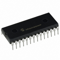
PIC16F57-I/P Microchip Technology, PIC16F57-I/P Datasheet - Page 37

PIC16F57-I/P
Manufacturer Part Number
PIC16F57-I/P
Description
IC MCU FLASH 2KX12 28DIP
Manufacturer
Microchip Technology
Series
PIC® 16Fr
Datasheets
1.PIC16F54-ISS.pdf
(88 pages)
2.PIC16F57-ISS.pdf
(16 pages)
3.PIC16F57-ISO.pdf
(86 pages)
Specifications of PIC16F57-I/P
Program Memory Type
FLASH
Program Memory Size
3KB (2K x 12)
Package / Case
28-DIP (0.600", 15.24mm)
Core Processor
PIC
Core Size
8-Bit
Speed
20MHz
Peripherals
POR, WDT
Number Of I /o
20
Ram Size
72 x 8
Voltage - Supply (vcc/vdd)
2 V ~ 5.5 V
Oscillator Type
External
Operating Temperature
-40°C ~ 85°C
Processor Series
PIC16F
Core
PIC
Data Bus Width
8 bit
Data Ram Size
72 B
Maximum Clock Frequency
20 MHz
Number Of Programmable I/os
20
Number Of Timers
1
Operating Supply Voltage
2 V to 5.5 V
Maximum Operating Temperature
+ 85 C
Mounting Style
Through Hole
3rd Party Development Tools
52715-96, 52716-328, 52717-734
Development Tools By Supplier
DV164120, DV164101, ICE2000
Minimum Operating Temperature
- 40 C
Data Rom Size
2 K
Height
3.3 mm
Length
34.67 mm
Supply Voltage (max)
5.5 V
Supply Voltage (min)
2 V
Width
7.24 mm
Lead Free Status / RoHS Status
Lead free / RoHS Compliant
For Use With
XLT28XP - SOCKET TRANSITION ICE 28DIPAC164001 - MODULE SKT PROMATEII 18/28DIP
Eeprom Size
-
Data Converters
-
Connectivity
-
Lead Free Status / Rohs Status
Lead free / RoHS Compliant
Available stocks
Company
Part Number
Manufacturer
Quantity
Price
Company:
Part Number:
PIC16F57-I/P
Manufacturer:
Microchip Technology
Quantity:
26 657
Part Number:
PIC16F57-I/P
Manufacturer:
MICROCHIP/微芯
Quantity:
20 000
7.1
When an external clock input is used for Timer0, it must
meet certain requirements. The external clock
requirement is due to internal phase clock (T
synchronization. Also, there is a delay in the actual
incrementing of Timer0 after synchronization.
7.1.1
When no prescaler is used, the external clock is the
Timer0 input. The synchronization of T0CKI with the
internal phase clocks is accomplished by sampling the
prescaler output on the Q2 and Q4 cycles of the inter-
nal phase clocks (Figure 7-4). Therefore, it is neces-
sary for T0CKI to be high for at least 2T
RC delay of 20 ns) and low for at least 2T
small RC delay of 20 ns). Refer to the electrical
specification of the desired device.
FIGURE 7-4:
7.2
An 8-bit counter is available as a prescaler for the
Timer0 module, or as a postscaler for the Watchdog
Timer (WDT), respectively (Section 8.2.1 “WDT
Period”). For simplicity, this counter is being referred
to as “prescaler” throughout this data sheet. Note that
the prescaler may be used by either the Timer0 module
or the WDT, but not both. Thus, a prescaler assignment
for the Timer0 module means that there is no prescaler
for the WDT, and vice-versa.
© 2007 Microchip Technology Inc.
Note 1:
2:
3:
Using Timer0 with an External
Clock
Prescaler
EXTERNAL CLOCK
SYNCHRONIZATION
External Clock/Prescaler
External clock if no prescaler selected; prescaler output otherwise.
The arrows indicate the points in time where sampling occurs.
Delay from clock input change to Timer0 increment is 3T
in measuring the interval between two edges on Timer0 input = ± 4T
External Clock Input or
Prescaler Output
Output After Sampling
Increment Timer0 (Q4)
TIMER0 TIMING WITH EXTERNAL CLOCK
Timer0
(1)
OSC
(2)
Q1 Q2 Q3 Q4
(and a small
OSC
(and a
(3)
OSC
)
Q1 Q2 Q3 Q4
T0
OSC
When a prescaler is used, the external clock input is
divided by the asynchronous ripple counter-type
prescaler so that the prescaler output is symmetrical.
For the external clock to meet the sampling require-
ment, the ripple counter must be taken into account.
Therefore, it is necessary for T0CKI to have a period of
at least 4T
by the prescaler value. The only requirement on T0CKI
high and low time is that they do not violate the
minimum pulse width requirement of 10 ns. Refer to
parameters 40, 41 and 42 in the electrical specification
of the desired device.
7.1.2
Since the prescaler output is synchronized with the
internal clocks, there is a small delay from the time the
external clock edge occurs to the time the Timer0
module is actually incremented. Figure 7-4 shows the
delay from the external clock edge to the timer
incrementing.
The PSA and PS<2:0> bits (OPTION<3:0>) determine
prescaler assignment and prescale ratio.
When assigned to the Timer0 module, all instructions
writing to the TMR0 register (e.g., CLRF 1, MOVWF 1,
BSF 1, x, etc.) will clear the prescaler. When assigned
to WDT, a CLRWDT instruction will clear the prescaler
along with the WDT. The prescaler is neither readable
nor writable. On a Reset, the prescaler contains all ‘0’s.
to 7T
OSC
OSC
OSC
Q1 Q2 Q3 Q4
TIMER0 INCREMENT DELAY
(duration of Q = T
T0 + 1
max.
(and a small RC delay of 40 ns) divided
OSC
PIC16F5X
Q1 Q2 Q3 Q4
). Therefore, the error
T0 + 2
Small pulse
misses sampling
DS41213D-page 35


