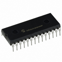
PIC16F57-I/P Microchip Technology, PIC16F57-I/P Datasheet - Page 41

PIC16F57-I/P
Manufacturer Part Number
PIC16F57-I/P
Description
IC MCU FLASH 2KX12 28DIP
Manufacturer
Microchip Technology
Series
PIC® 16Fr
Datasheets
1.PIC16F54-ISS.pdf
(88 pages)
2.PIC16F57-ISS.pdf
(16 pages)
3.PIC16F57-ISO.pdf
(86 pages)
Specifications of PIC16F57-I/P
Program Memory Type
FLASH
Program Memory Size
3KB (2K x 12)
Package / Case
28-DIP (0.600", 15.24mm)
Core Processor
PIC
Core Size
8-Bit
Speed
20MHz
Peripherals
POR, WDT
Number Of I /o
20
Ram Size
72 x 8
Voltage - Supply (vcc/vdd)
2 V ~ 5.5 V
Oscillator Type
External
Operating Temperature
-40°C ~ 85°C
Processor Series
PIC16F
Core
PIC
Data Bus Width
8 bit
Data Ram Size
72 B
Maximum Clock Frequency
20 MHz
Number Of Programmable I/os
20
Number Of Timers
1
Operating Supply Voltage
2 V to 5.5 V
Maximum Operating Temperature
+ 85 C
Mounting Style
Through Hole
3rd Party Development Tools
52715-96, 52716-328, 52717-734
Development Tools By Supplier
DV164120, DV164101, ICE2000
Minimum Operating Temperature
- 40 C
Data Rom Size
2 K
Height
3.3 mm
Length
34.67 mm
Supply Voltage (max)
5.5 V
Supply Voltage (min)
2 V
Width
7.24 mm
Lead Free Status / RoHS Status
Lead free / RoHS Compliant
For Use With
XLT28XP - SOCKET TRANSITION ICE 28DIPAC164001 - MODULE SKT PROMATEII 18/28DIP
Eeprom Size
-
Data Converters
-
Connectivity
-
Lead Free Status / Rohs Status
Lead free / RoHS Compliant
Available stocks
Company
Part Number
Manufacturer
Quantity
Price
Company:
Part Number:
PIC16F57-I/P
Manufacturer:
Microchip Technology
Quantity:
26 657
Part Number:
PIC16F57-I/P
Manufacturer:
MICROCHIP/微芯
Quantity:
20 000
8.3
A device may be powered down (Sleep) and later
powered up (wake-up from Sleep).
8.3.1
The Power-down mode is entered by executing a
SLEEP instruction.
If enabled, the Watchdog Timer will be cleared but
keeps running, the TO bit (STATUS<4>) is set, the PD
bit (STATUS<3>) is cleared and the oscillator driver is
turned off. The I/O ports maintain the status they had
before the SLEEP instruction was executed (driving
high, driving low or high-impedance).
It should be noted that a Reset generated by a WDT
time-out does not drive the MCLR/V
For lowest current consumption while powered down,
the T0CKI input should be at V
MCLR/V
(MCLR = V
8.3.2
The device can wake-up from Sleep through one of the
following events:
1.
2.
Both of these events cause a device Reset. The TO
and PD bits can be used to determine the cause of
device Reset. The TO bit is cleared if a WDT time-out
occurred (and caused wake-up). The PD bit, which is
set on power-up, is cleared when SLEEP is invoked.
The WDT is cleared when the device wakes from
Sleep, regardless of the wake-up source.
8.4
If the code protection bit has not been programmed, the
on-chip program memory can be read out for
verification purposes.
Once code protection is enabled, all program memory
locations above 0x3F read all ‘0’s. Program memory
locations 0x00-0x3F are always unprotected. The user
ID locations and the Configuration Word read out in an
unprotected fashion. It is possible to program the user
ID locations and the Configuration Word after code
protect is enabled.
© 2007 Microchip Technology Inc.
An external Reset input on MCLR/V
A Watchdog Timer time-out Reset (if WDT was
enabled).
PP
Power-Down Mode (Sleep)
Program Verification/Code
Protection
IH
pin must be at a logic high level
SLEEP
WAKE-UP FROM SLEEP
).
DD
PP
or V
pin low.
PP
SS
pin.
and the
8.5
Four memory locations are designated as user ID loca-
tions where the user can store checksum or other
code-identification numbers. These locations are not
accessible during normal execution, but are readable
and writable during Program/Verify.
Use only the lower 4 bits of the user ID locations and
always program the upper 8 bits as ‘1’s.
8.6
The PIC16F5X microcontrollers can be serially
programmed while in the end application circuit. This is
simply done with two lines for clock and data, and three
other lines for power, ground and programming
voltage. This allows customers to manufacture boards
with unprogrammed devices and then program the
microcontroller just before shipping the product. Thus,
the most recent firmware or custom firmware can be
programmed.
The device is placed into a Program/Verify mode by
holding the RB6 and RB7 pins low while raising the
MCLR (V
specification). RB6 becomes the programming clock
and RB7 becomes the programming data. Both RB6
and RB7 are Schmitt Trigger inputs in this mode.
A 6-bit command is then supplied to the device.
Depending on the command, 14 bits of program data
are then supplied to or from the device, depending if
the command was a Load or a Read. For complete
details of serial programming, please refer to the
respective Programming Specifications: “PIC16F54
Memory
“PIC16F57
(DS41208), and “PIC16F59 Memory Programming
Specification” (DS41243).
A typical In-Circuit Serial Programming connection is
shown in Figure 8-1.
Note:
User ID Locations
In-Circuit Serial Programming™
(ICSP™)
PP
Programming
Microchip will assign a unique pattern
number for QTP and SQTP requests. This
pattern number will be unique and trace-
able to the submitted code.
) pin from V
Memory
Programming
IL
Specification”
to V
PIC16F5X
IHH
(see programming
DS41213D-page 39
Specification”
(DS41207),


