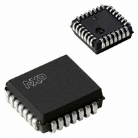
P89LPC9351FA,529 NXP Semiconductors, P89LPC9351FA,529 Datasheet - Page 31

P89LPC9351FA,529
Manufacturer Part Number
P89LPC9351FA,529
Description
IC 80C51 MCU FLASH 8K 28-PLCC
Manufacturer
NXP Semiconductors
Series
LPC900r
Datasheet
1.P89LPC9351FA112.pdf
(94 pages)
Specifications of P89LPC9351FA,529
Program Memory Type
FLASH
Program Memory Size
8KB (8K x 8)
Package / Case
28-PLCC
Core Processor
8051
Core Size
8-Bit
Speed
18MHz
Connectivity
I²C, SPI, UART/USART
Peripherals
Brown-out Detect/Reset, POR, PWM, Temp Sensor, WDT
Number Of I /o
26
Eeprom Size
512 x 8
Ram Size
768 x 8
Voltage - Supply (vcc/vdd)
2.4 V ~ 3.6 V
Data Converters
A/D 8x8b; D/A 2x8b
Oscillator Type
Internal
Operating Temperature
-40°C ~ 85°C
Processor Series
P89LPC
Core
80C51
Data Bus Width
8 bit
Data Ram Size
256 B
Interface Type
I2C, SPI, UART
Maximum Clock Frequency
18 MHz
Number Of Programmable I/os
23
Number Of Timers
2
Operating Supply Voltage
2.4 V to 3.6 V
Maximum Operating Temperature
+ 85 C
Mounting Style
SMD/SMT
3rd Party Development Tools
PK51, CA51, A51, ULINK2
Minimum Operating Temperature
- 40 C
On-chip Adc
8 bit, 8 Channel
Lead Free Status / RoHS Status
Lead free / RoHS Compliant
For Use With
OM11004 - KIT IAR KICKSTART LPC935568-1758 - BOARD EVAL FOR LPC93X MCU FAMILY
Lead Free Status / Rohs Status
Lead free / RoHS Compliant
Other names
935287627529
Available stocks
Company
Part Number
Manufacturer
Quantity
Price
Company:
Part Number:
P89LPC9351FA,529
Manufacturer:
NXP Semiconductors
Quantity:
10 000
NXP Semiconductors
P89LPC9331_9341_9351_9361
Product data sheet
7.5 Clock output
7.6 On-chip RC oscillator option
7.7 Watchdog oscillator option
7.8 External clock input option
7.9 Clock source switching on the fly
The P89LPC9331/9341/9351/9361 supports a user-selectable clock output function on
the XTAL2/CLKOUT pin when crystal oscillator is not being used. This condition occurs if
another clock source has been selected (on-chip RC oscillator, watchdog oscillator,
external clock input on XTAL1) and if the RTC and WDT are not using the crystal oscillator
as their clock source. This allows external devices to synchronize to the
P89LPC9331/9341/9351/9361. This output is enabled by the ENCLK bit in the TRIM
register.
The frequency of this clock output is
in Idle mode, it may be turned off prior to entering Idle, saving additional power.
The P89LPC9331/9341/9351/9361 has a 6-bit TRIM register that can be used to tune the
frequency of the RC oscillator. During reset, the TRIM value is initialized to a factory
preprogrammed value to adjust the oscillator frequency to 7.373 MHz ± 1 % at room
temperature. End-user applications can write to the TRIM register to adjust the on-chip
RC oscillator to other frequencies. When the clock doubler option is enabled (UCFG2.7 =
1), the output frequency is 14.746 MHz. If CCLK is 8 MHz or slower, the CLKLP SFR bit
(AUXR1.7) can be set to logic 1 to reduce power consumption. On reset, CLKLP is logic 0
allowing highest performance access. This bit can then be set in software if CCLK is
running at 8 MHz or slower. When clock doubler option is enabled, BOE1 bit (UCFG1.5)
and BOE0 bit (UCFG1.3) are required to hold the device in reset at power-up until V
has reached its specified level.
The watchdog has a separate oscillator which has a frequency of 400 kHz, calibrated to
±5 % at room temperature. This oscillator can be used to save power when a high clock
frequency is not needed.
In this configuration, the processor clock is derived from an external source driving the
P3.1/XTAL1 pin. The rate may be from 0 Hz up to 18 MHz. The P3.0/XTAL2 pin may be
used as a standard port pin or a clock output. When using an oscillator frequency above
12 MHz, BOE1 bit (UCFG1.5) and BOE0 bit (UCFG1.3) are required to hold the device in
reset at power-up until V
P89LPC9331/9341/9351/9361 can implement clock switching on any sources of
watchdog oscillator, 7 MHz/14 MHz internal RC oscillator, crystal oscillator and external
clock input during code is running. CLKOK bit in CLKCON register is used to indicate the
clock switch status. CLKOK is cleared when starting clock source switch and set when
completed. Notice that when CLKOK is ‘0’, writing to CLKCON register is not allowed.
All information provided in this document is subject to legal disclaimers.
Rev. 5 — 10 January 2011
DD
8-bit microcontroller with accelerated two-clock 80C51 core
has reached its specified level.
P89LPC9331/9341/9351/9361
1
⁄
2
that of the CCLK. If the clock output is not needed
© NXP B.V. 2011. All rights reserved.
31 of 94
DD


