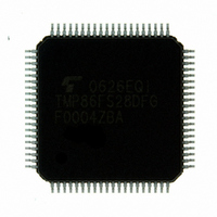
TMP86FS28DFG(JZ) Toshiba, TMP86FS28DFG(JZ) Datasheet - Page 211

TMP86FS28DFG(JZ)
Manufacturer Part Number
TMP86FS28DFG(JZ)
Description
IC MCU 8BIT FLASH 60KB 80-LQFP
Manufacturer
Toshiba
Series
TLCS-870/Cr
Datasheet
1.TMP86FS28DFGJZ.pdf
(272 pages)
Specifications of TMP86FS28DFG(JZ)
Core Processor
870/C
Core Size
8-Bit
Speed
16MHz
Connectivity
SIO, UART/USART
Peripherals
LCD, PWM, WDT
Number Of I /o
62
Program Memory Size
60KB (60K x 8)
Program Memory Type
FLASH
Ram Size
2K x 8
Voltage - Supply (vcc/vdd)
2.7 V ~ 5.5 V
Data Converters
A/D 8x10b
Oscillator Type
Internal
Operating Temperature
-40°C ~ 85°C
Package / Case
80-LQFP
Processor Series
TLCS-870
Core
870/C
Data Bus Width
8 bit
Data Ram Size
2 KB
Interface Type
SIO, UART
Maximum Clock Frequency
16 MHz
Number Of Programmable I/os
62
Number Of Timers
6
Maximum Operating Temperature
+ 85 C
Mounting Style
SMD/SMT
Development Tools By Supplier
BM1040R0A, BMP86A100010A, BMP86A100010B, BMP86A200010B, BMP86A200020A, BMP86A300010A, BMP86A300020A, BMP86A300030A, SW89CN0-ZCC, SW00MN0-ZCC
Minimum Operating Temperature
- 40 C
On-chip Adc
10 bit, 8 Channel
For Use With
BM1401W0A-G - FLASH WRITER ON-BOARD PROGRAMTMP89C900XBG - EMULATION CHIP TMP89F LQFP
Lead Free Status / RoHS Status
Lead free / RoHS Compliant
Eeprom Size
-
Lead Free Status / Rohs Status
Details
Other names
TMP86FS28DFGJZ
Available stocks
Company
Part Number
Manufacturer
Quantity
Price
- Current page: 211 of 272
- Download datasheet (3Mb)
16.3 LCD Display Operation
16.3.1 Display data setting
1/3 Bias (R1 = R2 = R3)
Keep the following conditon.
VDD
VSS
Figure 16-4 Connection Examples When Using an External Resistor Divider
The display data which are stored in the display data area is automatically read out and sent to the LCD driver
by the hardware. The LCD driver generates the segment signal and common signal according to the display
data and driving method. Therefore, display patterns can be changed by only over writing the contents of dis-
play data area by the program. Table 16-5 shows the correspondence between the display data area and SEG/
COM pins.
number of pixels which can be driven becomes different, and the number of bits in the display data area which
is used to store display data also becomes different.
addresses not connected to LCD can be used to store general user process data (see Table 16-4).
Display data is stored to the display data area (assigned to address 0FC0H to 0FD3H, 20bytes) in the DBR.
LCD light when display data is “1” and turn off when “0”. According to the driving method of LCD, the
Therefore, the bits which are not used to store display data as well as the data buffer which corresponds to the
Note:The display data memory contents become unstable when the power supply is turned on; therefore, the dis-
V DD
sumption is increased. Conversely, the larger the external resistor value, the lower the segment/common
drive capability, but power consumption is reduced. If the drive capability is insufficient, the LCD may
not be displayed clearly. Therefore, select an optimum resistor value for the LCD panel to be used.
The smaller the external resistor value, the higher the segment/common drive capability, but power con-
play data memory should be initialized by an initiation routine.
Adjustment of
C0
C1
V3
V2
V1
V 3
Table 16-4 Driving Method and Bit for Display Data
contrast
Open
Open
V 2
Driving methods
V 1
1/4 Duty
1/3 Duty
1/2 Duty
Static
R1
R2
R3
V SS
(LCDCR<BRES> = “0”)
1/2 Bias (R1 = R2)
VDD
VSS
Bit 7/3
COM3
–
–
–
Page 199
Adjustment of
V3
V2
C0
C1
V1
Bit 6/2
COM2
COM2
–
–
contrast
Open
Open
Bit 5/1
COM1
COM1
COM1
R1
R2
–
Bit 4/0
COM0
COM0
COM0
COM0
VDD
VSS
Static
Adjustment of
TMP86FS28DFG
C0
C1
V3
V2
V1
contrast
Open
Open
R1
Related parts for TMP86FS28DFG(JZ)
Image
Part Number
Description
Manufacturer
Datasheet
Request
R
Part Number:
Description:
Toshiba Semiconductor [TOSHIBA IGBT Module Silicon N Channel IGBT]
Manufacturer:
TOSHIBA Semiconductor CORPORATION
Datasheet:
Part Number:
Description:
TOSHIBA GTR MODULE SILICON NPN TRIPLE DIFFUSED TYPE
Manufacturer:
TOSHIBA Semiconductor CORPORATION
Datasheet:
Part Number:
Description:
TOSHIBA GTR Module Silicon N Channel IGBT
Manufacturer:
TOSHIBA Semiconductor CORPORATION
Datasheet:
Part Number:
Description:
TOSHIBA Intelligent Power Module Silicon N Channel IGBT
Manufacturer:
TOSHIBA Semiconductor CORPORATION
Datasheet:
Part Number:
Description:
TOSHIBA INTELLIGENT POWER MODULE SILICON N CHANNEL LGBT
Manufacturer:
TOSHIBA Semiconductor CORPORATION
Datasheet:
Part Number:
Description:
TOSHIBA IGBT Module Silicon N Channel IGBT
Manufacturer:
TOSHIBA Semiconductor CORPORATION
Datasheet:
Part Number:
Description:
TOSHIBA GTR MODULE SILICON N−CHANNEL IGBT
Manufacturer:
TOSHIBA Semiconductor CORPORATION
Datasheet:
Part Number:
Description:
TOSHIBA Intelligent Power Module Silicon N Channel IGBT
Manufacturer:
TOSHIBA Semiconductor CORPORATION
Datasheet:
Part Number:
Description:
TOSHIBA GTR Module Silicon N Channel IGBT
Manufacturer:
TOSHIBA Semiconductor CORPORATION
Datasheet:
Part Number:
Description:
TOSHIBA INTELLIGENT POWER MODULE
Manufacturer:
TOSHIBA Semiconductor CORPORATION
Datasheet:
Part Number:
Description:
TOSHIBA Intelligent Power Module Silicon N Channel IGBT
Manufacturer:
TOSHIBA Semiconductor CORPORATION
Datasheet:
Part Number:
Description:
TOSHIBA Intelligent Power Module Silicon N Channel IGBT
Manufacturer:
TOSHIBA Semiconductor CORPORATION
Datasheet:
Part Number:
Description:
TOSHIBA IGBT Module Silicon N Channel IGBT
Manufacturer:
TOSHIBA Semiconductor CORPORATION
Datasheet:
Part Number:
Description:
TOSHIBA Intelligent Power Module Silicon N Channel IGBT
Manufacturer:
TOSHIBA Semiconductor CORPORATION
Datasheet:
Part Number:
Description:
Toshiba Semiconductor [SILICON N CHANNEL 1GBT]
Manufacturer:
TOSHIBA Semiconductor CORPORATION
Datasheet:


