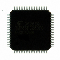
TMP86FS28DFG(JZ) Toshiba, TMP86FS28DFG(JZ) Datasheet - Page 222

TMP86FS28DFG(JZ)
Manufacturer Part Number
TMP86FS28DFG(JZ)
Description
IC MCU 8BIT FLASH 60KB 80-LQFP
Manufacturer
Toshiba
Series
TLCS-870/Cr
Datasheet
1.TMP86FS28DFGJZ.pdf
(272 pages)
Specifications of TMP86FS28DFG(JZ)
Core Processor
870/C
Core Size
8-Bit
Speed
16MHz
Connectivity
SIO, UART/USART
Peripherals
LCD, PWM, WDT
Number Of I /o
62
Program Memory Size
60KB (60K x 8)
Program Memory Type
FLASH
Ram Size
2K x 8
Voltage - Supply (vcc/vdd)
2.7 V ~ 5.5 V
Data Converters
A/D 8x10b
Oscillator Type
Internal
Operating Temperature
-40°C ~ 85°C
Package / Case
80-LQFP
Processor Series
TLCS-870
Core
870/C
Data Bus Width
8 bit
Data Ram Size
2 KB
Interface Type
SIO, UART
Maximum Clock Frequency
16 MHz
Number Of Programmable I/os
62
Number Of Timers
6
Maximum Operating Temperature
+ 85 C
Mounting Style
SMD/SMT
Development Tools By Supplier
BM1040R0A, BMP86A100010A, BMP86A100010B, BMP86A200010B, BMP86A200020A, BMP86A300010A, BMP86A300020A, BMP86A300030A, SW89CN0-ZCC, SW00MN0-ZCC
Minimum Operating Temperature
- 40 C
On-chip Adc
10 bit, 8 Channel
For Use With
BM1401W0A-G - FLASH WRITER ON-BOARD PROGRAMTMP89C900XBG - EMULATION CHIP TMP89F LQFP
Lead Free Status / RoHS Status
Lead free / RoHS Compliant
Eeprom Size
-
Lead Free Status / Rohs Status
Details
Other names
TMP86FS28DFGJZ
Available stocks
Company
Part Number
Manufacturer
Quantity
Price
- Current page: 222 of 272
- Download datasheet (3Mb)
17.1 Flash Memory Control
17.1 Flash Memory Control
Flash Memory Control Register
Flash Memory Standby Control Register
(0FADH)
17.1.1 Flash Memory Command Sequence Execution Control (FLSCR<FLSMD>)
17.1.2 Flash Memory Bank Select Control (FLSCR<BANKSEL>)
(0FAFH)
FLSSTB
FLSCR
resister (FLSSTB).
The flash memory is controlled via the flash memory control register (FLSCR) and flash memory stanby control
Note 1: The command sequence of the flash memory can be executed only when FLSMD="0011B". In other cases, any attempts
Note 2: FLSMD must be set to either "1100B" or "0011B".
Note 3: BANKSEL is effective only in the serial PROM mode. In the MCU mode, the flash memory is always accessed with actual
Note 4: Bits 2 through 0 in FLSCR are always read as don’t care.
Note 1: When FSTB is set to 1, do not execute the read/write instruction to the flash memory because there is a possibility that the
Note 2: If an interrupt is issued when FSTB is set to 1, FSTB is initialized to 0 automatically and then the vector area of the flash
Note 3: If the IDLE0/1/2, SLEEP0/1/2 or STOP mode is activated when FSTB is set to 1, FSTB is initialized to 0 automatically. In
ation. This write protection feature is realized by disabling flash memory command sequence execution via the
flash memory control register (write protect). To enable command sequence execution, set FLSCR<FLSMD>
to “0011B”. To disable command sequence execution, set FLSCR<FLSMD> to “1100B”. After reset,
FLSCR<FLSMD> is initialized to “1100B” to disable command sequence execution. Normally,
FLSCR<FLSMD> should be set to “1100B” except when the flash memory needs to be written or erased.
ory is mapped to 2 banks at 8000H-FFFFH. Flash memory addresses 1000H-7FFFH are mapped to 9000H-
FFFFH as BANK0, and flash memory addresses 8000H-FFFFH are mapped to 8000H-FFFFH as BANK1.
FLSCR<BANKSEL> is used to switch between these banks. For example, to access the flash memory address
7000H, set FLSCR<BANKSEL> to “0” and then access F000H. To access the flash memory address 9000H,
set FLSCR<BANKSEL> to “1" and then access 9000H.
FLSCR<BANKSEL> is ineffective (i.e., its value has no effect on other operations).
BANKSEL
The flash memory can be protected from inadvertent write due to program error or microcontroller misoper-
In the serial PROM mode, a 2-kbyte BOOTROM is mapped to addresses 7800H-7FFFH and the flash mem-
In the MCU mode, the flash memory is accessed with actual addresses at 1000H-FFFFH. In this case,
FLSMD
to execute the command sequence are ineffective.
addresses (1000-FFFFH) regardless of BANKSEL.
expected data is not read or the program is not operated correctly. If executing the read/write instruction, FSTB is initial-
ized to 0 automatically.
memory is read.
the IDLE0/1/2, SLEEP0/1/2 or STOP mode, the standby function operates regardless of FSTB setting.
FSTB
7
7
Flash memory command sequence exe-
cution control
Flash memory bank select control
(Serial PROM mode only)
Flash memory standby control
6
6
FLSMD
5
5
4
4
BANKSEL
Page 210
3
3
1100: Disable command sequence execution
0011: Enable command sequence execution
Others: Reserved
0: Select BANK0
1: Select BANK1
0: Disable the standby function.
1: Enable the standby function.
2
2
1
1
FSTB
0
0
(Initial value : 1100 1***)
(Initial value : **** ***0)
TMP86FS28DFG
Write
R/W
R/W
only
Related parts for TMP86FS28DFG(JZ)
Image
Part Number
Description
Manufacturer
Datasheet
Request
R
Part Number:
Description:
Toshiba Semiconductor [TOSHIBA IGBT Module Silicon N Channel IGBT]
Manufacturer:
TOSHIBA Semiconductor CORPORATION
Datasheet:
Part Number:
Description:
TOSHIBA GTR MODULE SILICON NPN TRIPLE DIFFUSED TYPE
Manufacturer:
TOSHIBA Semiconductor CORPORATION
Datasheet:
Part Number:
Description:
TOSHIBA GTR Module Silicon N Channel IGBT
Manufacturer:
TOSHIBA Semiconductor CORPORATION
Datasheet:
Part Number:
Description:
TOSHIBA Intelligent Power Module Silicon N Channel IGBT
Manufacturer:
TOSHIBA Semiconductor CORPORATION
Datasheet:
Part Number:
Description:
TOSHIBA INTELLIGENT POWER MODULE SILICON N CHANNEL LGBT
Manufacturer:
TOSHIBA Semiconductor CORPORATION
Datasheet:
Part Number:
Description:
TOSHIBA IGBT Module Silicon N Channel IGBT
Manufacturer:
TOSHIBA Semiconductor CORPORATION
Datasheet:
Part Number:
Description:
TOSHIBA GTR MODULE SILICON N−CHANNEL IGBT
Manufacturer:
TOSHIBA Semiconductor CORPORATION
Datasheet:
Part Number:
Description:
TOSHIBA Intelligent Power Module Silicon N Channel IGBT
Manufacturer:
TOSHIBA Semiconductor CORPORATION
Datasheet:
Part Number:
Description:
TOSHIBA GTR Module Silicon N Channel IGBT
Manufacturer:
TOSHIBA Semiconductor CORPORATION
Datasheet:
Part Number:
Description:
TOSHIBA INTELLIGENT POWER MODULE
Manufacturer:
TOSHIBA Semiconductor CORPORATION
Datasheet:
Part Number:
Description:
TOSHIBA Intelligent Power Module Silicon N Channel IGBT
Manufacturer:
TOSHIBA Semiconductor CORPORATION
Datasheet:
Part Number:
Description:
TOSHIBA Intelligent Power Module Silicon N Channel IGBT
Manufacturer:
TOSHIBA Semiconductor CORPORATION
Datasheet:
Part Number:
Description:
TOSHIBA IGBT Module Silicon N Channel IGBT
Manufacturer:
TOSHIBA Semiconductor CORPORATION
Datasheet:
Part Number:
Description:
TOSHIBA Intelligent Power Module Silicon N Channel IGBT
Manufacturer:
TOSHIBA Semiconductor CORPORATION
Datasheet:
Part Number:
Description:
Toshiba Semiconductor [SILICON N CHANNEL 1GBT]
Manufacturer:
TOSHIBA Semiconductor CORPORATION
Datasheet:


