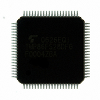
TMP86FS28DFG(JZ) Toshiba, TMP86FS28DFG(JZ) Datasheet - Page 264

TMP86FS28DFG(JZ)
Manufacturer Part Number
TMP86FS28DFG(JZ)
Description
IC MCU 8BIT FLASH 60KB 80-LQFP
Manufacturer
Toshiba
Series
TLCS-870/Cr
Datasheet
1.TMP86FS28DFGJZ.pdf
(272 pages)
Specifications of TMP86FS28DFG(JZ)
Core Processor
870/C
Core Size
8-Bit
Speed
16MHz
Connectivity
SIO, UART/USART
Peripherals
LCD, PWM, WDT
Number Of I /o
62
Program Memory Size
60KB (60K x 8)
Program Memory Type
FLASH
Ram Size
2K x 8
Voltage - Supply (vcc/vdd)
2.7 V ~ 5.5 V
Data Converters
A/D 8x10b
Oscillator Type
Internal
Operating Temperature
-40°C ~ 85°C
Package / Case
80-LQFP
Processor Series
TLCS-870
Core
870/C
Data Bus Width
8 bit
Data Ram Size
2 KB
Interface Type
SIO, UART
Maximum Clock Frequency
16 MHz
Number Of Programmable I/os
62
Number Of Timers
6
Maximum Operating Temperature
+ 85 C
Mounting Style
SMD/SMT
Development Tools By Supplier
BM1040R0A, BMP86A100010A, BMP86A100010B, BMP86A200010B, BMP86A200020A, BMP86A300010A, BMP86A300020A, BMP86A300030A, SW89CN0-ZCC, SW00MN0-ZCC
Minimum Operating Temperature
- 40 C
On-chip Adc
10 bit, 8 Channel
For Use With
BM1401W0A-G - FLASH WRITER ON-BOARD PROGRAMTMP89C900XBG - EMULATION CHIP TMP89F LQFP
Lead Free Status / RoHS Status
Lead free / RoHS Compliant
Eeprom Size
-
Lead Free Status / Rohs Status
Details
Other names
TMP86FS28DFGJZ
Available stocks
Company
Part Number
Manufacturer
Quantity
Price
- Current page: 264 of 272
- Download datasheet (3Mb)
20.3 DC Characteristics
20.3 DC Characteristics
Hysteresis voltage
Input current
Input resistance
Output leakage current
Output high voltage
Output low voltage
Supply current in
NORMAL 1, 2 mode
Supply current in
IDLE 0, 1, 2 mode
Supply current in
SLOW 1 mode
Supply current in
SLEEP 1 mode
Supply current in
SLEEP 0 mode
Supply current in
STOP mode
LCD output voltage
use LCD driver’s
Program coutner (PC)
Parameter
booste
Note 1: Typical values show those at Topr = 25°C, V
Note 2: Input current (I
Note 3: I
Note 4: The supply currents of SLOW 2 and SLEEP 2 modes are equivalent to IDLE 0, 1, 2.
Note 5: When a program is executing in the flash memory or when data is being read from the flash memory, the flash memory
Note 6: When designing the power supply, make sure that peak currents can be supplied. In SLOW1 mode, the difference
operates in an intermittent manner, causing peak currents in the operation current, as shown in Figure 20-1.
In this case, the supply current I
peak current and MCU current.
between the peak current and the average current becomes large.
DD
does not include I
I
V
DDP-P
Symbol
2-3OUT
R
V
V
V
[mA]
I
I
I
I
I
IN1
IN2
IN3
DD
LO
IN2
OH
HS
OL
Figure 20-1 Intermittent Operation of Flash Memory
IN1
, I
1 machine cycle (4/fc or 4/fs)
Hysteresis input
TEST
Sink open drain, Tri-state
RESET
RESET
Sink open drain, Tri-state
C-MOS, Tri-st port
Except XOUT
V2 terminal
V3 terminal
IN2
n
REF
); The current through pull-up or pull-down resistor is not included.
,
pull-up
STOP
current.
Pins
DD
n+1
(in NORMAL1, NORMAL2 and SLOW1 modes) is defined as the sum of the average
n+2
DD
V
V
V
V
V
V3 ≥ V
Reference supply terminal :V1
SEG/COM terminal no load
V
V
fc = 16 MHz
fs = 32.768 kHz
V
V
fs = 32.768 kHz
LCD drive is not
enable.
V
V
DD
DD
DD
DD
DD
DD
IN
DD
IN
DD
IN
Page 252
= 5 V
= 5.3/0.2 V
= 2.8/0.2 V
= 5.3 V/0.2 V
= 5.5 V, V
= 5.5 V, V
= 5.5 V, V
= 4.5 V, I
= 4.5 V, I
= 5.5 V
= 3.0 V
= 5.5 V
DD
n+3
OH
OL
IN
IN
OUT
Condition
= 1.6 mA
= 5.5 V/0 V
= 0 V
= −0.7 mA
= 5.5 V/0 V
When a program
operates on flash
memory (Note5,6)
When a program
operates on flash
memory (Note5,6)
When a program
operates on RAM
Momentary flash current
Max. current
Typ. current
MCU current
Min
100
4.1
–
–
–
–
–
–
–
–
–
–
–
–
–
Sum of average
momentary flash current
and MCU current
(V
V1 x 2
V1 x 3
SS
15.5
Typ.
220
0.9
0.5
25
20
–
–
–
–
6
9
8
= 0 V, Topr = −40 to 85°C)
TMP86FS28DFG
Max
16.5
450
260
0.4
8.3
±2
±2
24
21
18
10
–
–
–
–
Unit
mA
µA
kΩ
µA
µA
V
V
V
Related parts for TMP86FS28DFG(JZ)
Image
Part Number
Description
Manufacturer
Datasheet
Request
R
Part Number:
Description:
Toshiba Semiconductor [TOSHIBA IGBT Module Silicon N Channel IGBT]
Manufacturer:
TOSHIBA Semiconductor CORPORATION
Datasheet:
Part Number:
Description:
TOSHIBA GTR MODULE SILICON NPN TRIPLE DIFFUSED TYPE
Manufacturer:
TOSHIBA Semiconductor CORPORATION
Datasheet:
Part Number:
Description:
TOSHIBA GTR Module Silicon N Channel IGBT
Manufacturer:
TOSHIBA Semiconductor CORPORATION
Datasheet:
Part Number:
Description:
TOSHIBA Intelligent Power Module Silicon N Channel IGBT
Manufacturer:
TOSHIBA Semiconductor CORPORATION
Datasheet:
Part Number:
Description:
TOSHIBA INTELLIGENT POWER MODULE SILICON N CHANNEL LGBT
Manufacturer:
TOSHIBA Semiconductor CORPORATION
Datasheet:
Part Number:
Description:
TOSHIBA IGBT Module Silicon N Channel IGBT
Manufacturer:
TOSHIBA Semiconductor CORPORATION
Datasheet:
Part Number:
Description:
TOSHIBA GTR MODULE SILICON N−CHANNEL IGBT
Manufacturer:
TOSHIBA Semiconductor CORPORATION
Datasheet:
Part Number:
Description:
TOSHIBA Intelligent Power Module Silicon N Channel IGBT
Manufacturer:
TOSHIBA Semiconductor CORPORATION
Datasheet:
Part Number:
Description:
TOSHIBA GTR Module Silicon N Channel IGBT
Manufacturer:
TOSHIBA Semiconductor CORPORATION
Datasheet:
Part Number:
Description:
TOSHIBA INTELLIGENT POWER MODULE
Manufacturer:
TOSHIBA Semiconductor CORPORATION
Datasheet:
Part Number:
Description:
TOSHIBA Intelligent Power Module Silicon N Channel IGBT
Manufacturer:
TOSHIBA Semiconductor CORPORATION
Datasheet:
Part Number:
Description:
TOSHIBA Intelligent Power Module Silicon N Channel IGBT
Manufacturer:
TOSHIBA Semiconductor CORPORATION
Datasheet:
Part Number:
Description:
TOSHIBA IGBT Module Silicon N Channel IGBT
Manufacturer:
TOSHIBA Semiconductor CORPORATION
Datasheet:
Part Number:
Description:
TOSHIBA Intelligent Power Module Silicon N Channel IGBT
Manufacturer:
TOSHIBA Semiconductor CORPORATION
Datasheet:
Part Number:
Description:
Toshiba Semiconductor [SILICON N CHANNEL 1GBT]
Manufacturer:
TOSHIBA Semiconductor CORPORATION
Datasheet:


