R5F21324ANSP#U1 Renesas Electronics America, R5F21324ANSP#U1 Datasheet - Page 32
R5F21324ANSP#U1
Manufacturer Part Number
R5F21324ANSP#U1
Description
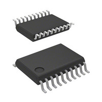
MCU 1KB FLASH 16K ROM 20-LSSOP
Manufacturer
Renesas Electronics America
Series
R8C/3x/32Ar
Datasheet
1.R5F21322ANSPU1.pdf
(629 pages)
Specifications of R5F21324ANSP#U1
Core Processor
R8C
Core Size
16/32-Bit
Speed
20MHz
Connectivity
I²C, LIN, SIO, SSU, UART/USART
Peripherals
POR, PWM, Voltage Detect, WDT
Number Of I /o
15
Program Memory Size
16KB (16K x 8)
Program Memory Type
FLASH
Ram Size
1.5K x 8
Voltage - Supply (vcc/vdd)
1.8 V ~ 5.5 V
Data Converters
A/D 4x10b
Oscillator Type
Internal
Operating Temperature
-20°C ~ 85°C
Package / Case
20-LSSOP
Lead Free Status / RoHS Status
Lead free / RoHS Compliant
Eeprom Size
-
Available stocks
Company
Part Number
Manufacturer
Quantity
Price


Under development
R8C/32A Group
REJ09B0458-0020 Rev.0.20
Page 2 of 583
1.1.2
Table 1.1
CPU
Memory
Power Supply
Voltage
Detection
I/O Ports
Clock
Interrupts
Watchdog Timer
DTC (Data Transfer Controller)
Timer
Item
Tables 1.1 and 1.2 outline the Specifications for R8C/32A Group.
Specifications
Preliminary specification
Specifications in this manual are tentative and subject to change.
Specifications for R8C/32A Group (1)
Central processing
unit
ROM, RAM, Data
flash
Voltage detection
circuit
Programmable I/O
ports
Clock generation
circuits
Timer RA
Timer RB
Timer RC
Timer RE
Function
Nov 05, 2008
R8C CPU core
• Number of fundamental instructions: 89
• Minimum instruction execution time:
• Multiplier: 16 bits × 16 bits → 32 bits
• Multiply-accumulate instruction: 16 bits × 16 bits + 32 bits → 32 bits
• Operation mode: Single-chip mode (address space: 1 Mbyte)
Refer to Table 1.3 Product List for R8C/32A Group.
• Power-on reset
• Voltage detection 3 (detection level of voltage detection 0 and voltage
• Input-only: 1 pin
• CMOS I/O ports: 15, selectable pull-up resistor
• High current drive ports: 15
4 circuits: XIN clock oscillation circuit,
• Oscillation stop detection: XIN clock oscillation stop detection function
• Frequency divider circuit: Dividing selectable 1, 2, 4, 8, and 16
• Low power consumption modes:
Real-time clock (timer RE)
• Number of interrupt vectors: 69
• External Interrupt: 7 (INT × 3, Key input × 4)
• Priority levels: 7 levels
• 14 bits × 1 (with prescaler)
• Reset start selectable
• Low-speed on-chip oscillator for watchdog timer selectable
• 1 channel
• Activation sources: 21
• Transfer modes: 2 (normal mode, repeat mode)
8 bits × 1 (with 8-bit prescaler)
8 bits × 1 (with 8-bit prescaler)
16 bits × 1 (with 4 capture/compare registers)
8 bits × 1
detection 1 selectable)
Timer mode (period timer), pulse output mode (output level inverted every
period), event counter mode, pulse width measurement mode, pulse period
measurement mode
Timer mode (period timer), programmable waveform generation mode (PWM
output), programmable one-shot generation mode, programmable wait one-
shot generation mode
Timer mode (input capture function, output compare function), PWM mode
(output 3 pins), PWM2 mode (PWM output pin)
Real-time clock mode (count seconds, minutes, hours, days of week), output
compare mode
Standard operating mode (high-speed clock, low-speed clock, high-speed
on-chip oscillator, low-speed on-chip oscillator), wait mode, stop mode
50 ns (f(XIN) = 20 MHz, VCC = 2.7 to 5.5 V)
200 ns (f(XIN) = 5 MHz, VCC = 1.8 to 5.5 V)
XCIN clock oscillation circuit (32 kHz)
High-speed on-chip oscillator (with frequency adjustment function),
Low-speed on-chip oscillator,
Specification
1. Overview
Related parts for R5F21324ANSP#U1
Image
Part Number
Description
Manufacturer
Datasheet
Request
R

Part Number:
Description:
KIT STARTER FOR M16C/29
Manufacturer:
Renesas Electronics America
Datasheet:

Part Number:
Description:
KIT STARTER FOR R8C/2D
Manufacturer:
Renesas Electronics America
Datasheet:

Part Number:
Description:
R0K33062P STARTER KIT
Manufacturer:
Renesas Electronics America
Datasheet:

Part Number:
Description:
KIT STARTER FOR R8C/23 E8A
Manufacturer:
Renesas Electronics America
Datasheet:

Part Number:
Description:
KIT STARTER FOR R8C/25
Manufacturer:
Renesas Electronics America
Datasheet:

Part Number:
Description:
KIT STARTER H8S2456 SHARPE DSPLY
Manufacturer:
Renesas Electronics America
Datasheet:

Part Number:
Description:
KIT STARTER FOR R8C38C
Manufacturer:
Renesas Electronics America
Datasheet:

Part Number:
Description:
KIT STARTER FOR R8C35C
Manufacturer:
Renesas Electronics America
Datasheet:

Part Number:
Description:
KIT STARTER FOR R8CL3AC+LCD APPS
Manufacturer:
Renesas Electronics America
Datasheet:
Part Number:
Description:
KIT STARTER FOR RX610
Manufacturer:
Renesas Electronics America
Datasheet:

Part Number:
Description:
KIT STARTER FOR R32C/118
Manufacturer:
Renesas Electronics America
Datasheet:

Part Number:
Description:
KIT DEV RSK-R8C/26-29
Manufacturer:
Renesas Electronics America
Datasheet:

Part Number:
Description:
KIT STARTER FOR SH7124
Manufacturer:
Renesas Electronics America
Datasheet:

Part Number:
Description:
KIT STARTER FOR H8SX/1622
Manufacturer:
Renesas Electronics America
Datasheet:

Part Number:
Description:
KIT DEV FOR SH7203
Manufacturer:
Renesas Electronics America
Datasheet: