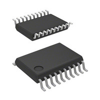
R5F21324ANSP#U1 Renesas Electronics America, R5F21324ANSP#U1 Datasheet - Page 436

R5F21324ANSP#U1
Manufacturer Part Number
R5F21324ANSP#U1
Description
MCU 1KB FLASH 16K ROM 20-LSSOP
Manufacturer
Renesas Electronics America
Series
R8C/3x/32Ar
Datasheet
1.R5F21322ANSPU1.pdf
(629 pages)
Specifications of R5F21324ANSP#U1
Core Processor
R8C
Core Size
16/32-Bit
Speed
20MHz
Connectivity
I²C, LIN, SIO, SSU, UART/USART
Peripherals
POR, PWM, Voltage Detect, WDT
Number Of I /o
15
Program Memory Size
16KB (16K x 8)
Program Memory Type
FLASH
Ram Size
1.5K x 8
Voltage - Supply (vcc/vdd)
1.8 V ~ 5.5 V
Data Converters
A/D 4x10b
Oscillator Type
Internal
Operating Temperature
-20°C ~ 85°C
Package / Case
20-LSSOP
Lead Free Status / RoHS Status
Lead free / RoHS Compliant
Eeprom Size
-
Available stocks
Company
Part Number
Manufacturer
Quantity
Price
- Current page: 436 of 629
- Download datasheet (7Mb)
Under development
R8C/32A Group
REJ09B0458-0020 Rev.0.20
Page 406 of 583
25.4
Figure 25.4
25.4.1
(1) I
(2) I
Legend:
S
SLA
R/W
A
DATA : Transmit/receive data
P
(a) I
(b) I
2
2
C bus format
C bus timing
When the FS bit in the SAR register is set to 0, the I
Figure 25.4 shows the I
8 bits.
: Start condition
: Slave address
: Indicates the direction of data transmission/reception
: Acknowledge
: Stop condition
2
2
C bus format (FS = 0)
C bus format When Start Condition is Retransmitted (FS = 0)
The master device changes the SDA signal from “H” to “L” while the SCL signal is held “H”.
Data is transmitted when:
R/W value is 1: From the slave device to the master device
R/W value is 0: From the master device to the slave device
The receive device sets the SDA signal to “L”.
The master device changes the SDA signal from “L” to “H” while the SCL signal is held “H”.
I
SDA
SCL
2
S
S
1
C bus Interface Mode
1
I
2
C bus Format
S
I
Preliminary specification
Specifications in this manual are tentative and subject to change.
2
C bus Format and Bus Timing
SLA
SLA
7
7
1 to 7
SLA
1
1
R/W
R/W
8
2
1
R/W
1
C bus Format and Bus Timing. The first frame following the start condition consists of
Nov 05, 2008
A
A
1
1
9
A
DATA
DATA
n
n1
1 to 7
m1
DATA
8
A
1
m
A/A
1
2
9
C bus format is used for communication.
A
S
1
A/A
1 to 7
1
SLA
7
P
1
DATA
1
8
Upper: Number of transfer bits (n1, n2 = 1 to 8)
Lower: Number of transfer frames (m1, m2 = 1 or more)
Number of transfer bits (n = 1 to 8)
Number of transfer frames (m = 1 or more)
R/W
1
9
A
A
1
P
DATA
n2
25. I
m2
2
C bus Interface
A/A
1
P
1
Related parts for R5F21324ANSP#U1
Image
Part Number
Description
Manufacturer
Datasheet
Request
R

Part Number:
Description:
KIT STARTER FOR M16C/29
Manufacturer:
Renesas Electronics America
Datasheet:

Part Number:
Description:
KIT STARTER FOR R8C/2D
Manufacturer:
Renesas Electronics America
Datasheet:

Part Number:
Description:
R0K33062P STARTER KIT
Manufacturer:
Renesas Electronics America
Datasheet:

Part Number:
Description:
KIT STARTER FOR R8C/23 E8A
Manufacturer:
Renesas Electronics America
Datasheet:

Part Number:
Description:
KIT STARTER FOR R8C/25
Manufacturer:
Renesas Electronics America
Datasheet:

Part Number:
Description:
KIT STARTER H8S2456 SHARPE DSPLY
Manufacturer:
Renesas Electronics America
Datasheet:

Part Number:
Description:
KIT STARTER FOR R8C38C
Manufacturer:
Renesas Electronics America
Datasheet:

Part Number:
Description:
KIT STARTER FOR R8C35C
Manufacturer:
Renesas Electronics America
Datasheet:

Part Number:
Description:
KIT STARTER FOR R8CL3AC+LCD APPS
Manufacturer:
Renesas Electronics America
Datasheet:

Part Number:
Description:
KIT STARTER FOR RX610
Manufacturer:
Renesas Electronics America
Datasheet:

Part Number:
Description:
KIT STARTER FOR R32C/118
Manufacturer:
Renesas Electronics America
Datasheet:

Part Number:
Description:
KIT DEV RSK-R8C/26-29
Manufacturer:
Renesas Electronics America
Datasheet:

Part Number:
Description:
KIT STARTER FOR SH7124
Manufacturer:
Renesas Electronics America
Datasheet:

Part Number:
Description:
KIT STARTER FOR H8SX/1622
Manufacturer:
Renesas Electronics America
Datasheet:

Part Number:
Description:
KIT DEV FOR SH7203
Manufacturer:
Renesas Electronics America
Datasheet:


