R5F21324ANSP#U1 Renesas Electronics America, R5F21324ANSP#U1 Datasheet - Page 525
R5F21324ANSP#U1
Manufacturer Part Number
R5F21324ANSP#U1
Description
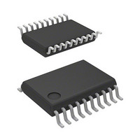
MCU 1KB FLASH 16K ROM 20-LSSOP
Manufacturer
Renesas Electronics America
Series
R8C/3x/32Ar
Datasheet
1.R5F21322ANSPU1.pdf
(629 pages)
Specifications of R5F21324ANSP#U1
Core Processor
R8C
Core Size
16/32-Bit
Speed
20MHz
Connectivity
I²C, LIN, SIO, SSU, UART/USART
Peripherals
POR, PWM, Voltage Detect, WDT
Number Of I /o
15
Program Memory Size
16KB (16K x 8)
Program Memory Type
FLASH
Ram Size
1.5K x 8
Voltage - Supply (vcc/vdd)
1.8 V ~ 5.5 V
Data Converters
A/D 4x10b
Oscillator Type
Internal
Operating Temperature
-20°C ~ 85°C
Package / Case
20-LSSOP
Lead Free Status / RoHS Status
Lead free / RoHS Compliant
Eeprom Size
-
Available stocks
Company
Part Number
Manufacturer
Quantity
Price


Under development
R8C/32A Group
REJ09B0458-0020 Rev.0.20
Page 495 of 583
FMSTP Bit (Flash Memory Stop Bit)
CMDRST Bit (Erase/Write Sequence Reset Bit)
CMDERIE Bit (Erase/Write Interrupt Enable Bit)
BSYAEIE Bit (Flash Access Error Interrupt Enable Bit)
RDYSTIE Bit (Flash Ready Status Interrupt Enable Bit)
This bit is used to initialize the flash memory control circuits, and also to reduce the amount of current
consumed by the flash memory. Access to the flash memory is disabled by setting the FMSTP bit to 1.
Write to the FMSTP bit by a program transferred to the RAM.
To reduce the power consumption further in high-speed on-chip oscillator mode, low-speed on-chip oscillator
mode (XIN clock stopped), and low-speed clock mode (XIN clock stopped), set the FMSTP bit to 1. Refer to
31.2.10 Stopping Flash Memory for details.
When entering stop mode or wait mode while CPU rewrite mode is disabled, the FMR0 register does not need
to be set because the power for the flash memory is automatically turned off and is turned back on when exiting
stop or wait mode.
This bit is used to initialize the flash memory sequence and forcibly stop a program or erase command. The user
ROM area can be read while the flash memory sequence is being initialized.
For addresses and blocks which the program or erase command is forcibly stopped by the CMDRST bit,
execute a block erasure again and ensure it completes normally. If the addresses and blocks which the program
or block erase command is forcibly stopped are allocated in the program area, set the FMR13 bit in the FMR1
register to 1 (lock bit disabled) before executing the block erasure command again.
The time from when the command is forcibly stopped and until reading is enabled is some hundreds µs where
the suspend response time is 10 ms.
This bit enables an flash command error interrupt to be generated if a program or block erase error occurs. If the
CMDERIE bit is set to 1 (erase/write error interrupt enabled) and erasure/writing is performed, an interrupt is
generated if an erase or program error occurs.
If a flash command error interrupt is generated, execute the clear status register command during interrupt
handling.
This bit enables a flash access error interrupt to be generated if the flash memory during rewriting is accessed.
This bit enables a flash ready status error interrupt to be generated when the status of the flash memory
sequence changes from the busy to ready status.
Preliminary specification
Specifications in this manual are tentative and subject to change.
Nov 05, 2008
30. Flash Memory
Related parts for R5F21324ANSP#U1
Image
Part Number
Description
Manufacturer
Datasheet
Request
R

Part Number:
Description:
KIT STARTER FOR M16C/29
Manufacturer:
Renesas Electronics America
Datasheet:

Part Number:
Description:
KIT STARTER FOR R8C/2D
Manufacturer:
Renesas Electronics America
Datasheet:

Part Number:
Description:
R0K33062P STARTER KIT
Manufacturer:
Renesas Electronics America
Datasheet:

Part Number:
Description:
KIT STARTER FOR R8C/23 E8A
Manufacturer:
Renesas Electronics America
Datasheet:

Part Number:
Description:
KIT STARTER FOR R8C/25
Manufacturer:
Renesas Electronics America
Datasheet:

Part Number:
Description:
KIT STARTER H8S2456 SHARPE DSPLY
Manufacturer:
Renesas Electronics America
Datasheet:

Part Number:
Description:
KIT STARTER FOR R8C38C
Manufacturer:
Renesas Electronics America
Datasheet:

Part Number:
Description:
KIT STARTER FOR R8C35C
Manufacturer:
Renesas Electronics America
Datasheet:

Part Number:
Description:
KIT STARTER FOR R8CL3AC+LCD APPS
Manufacturer:
Renesas Electronics America
Datasheet:
Part Number:
Description:
KIT STARTER FOR RX610
Manufacturer:
Renesas Electronics America
Datasheet:

Part Number:
Description:
KIT STARTER FOR R32C/118
Manufacturer:
Renesas Electronics America
Datasheet:

Part Number:
Description:
KIT DEV RSK-R8C/26-29
Manufacturer:
Renesas Electronics America
Datasheet:

Part Number:
Description:
KIT STARTER FOR SH7124
Manufacturer:
Renesas Electronics America
Datasheet:

Part Number:
Description:
KIT STARTER FOR H8SX/1622
Manufacturer:
Renesas Electronics America
Datasheet:

Part Number:
Description:
KIT DEV FOR SH7203
Manufacturer:
Renesas Electronics America
Datasheet: