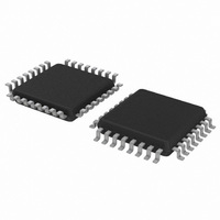
C8051F930-GQ Silicon Laboratories Inc, C8051F930-GQ Datasheet - Page 114

C8051F930-GQ
Manufacturer Part Number
C8051F930-GQ
Description
IC 8051 MCU 64K FLASH 32-LQFP
Manufacturer
Silicon Laboratories Inc
Series
C8051F9xxr
Specifications of C8051F930-GQ
Program Memory Type
FLASH
Program Memory Size
64KB (64K x 8)
Package / Case
32-LQFP
Core Processor
8051
Core Size
8-Bit
Speed
25MHz
Connectivity
SMBus (2-Wire/I²C), SPI, UART/USART
Peripherals
Brown-out Detect/Reset, POR, PWM, Temp Sensor, WDT
Number Of I /o
24
Ram Size
4.25K x 8
Voltage - Supply (vcc/vdd)
0.9 V ~ 3.6 V
Data Converters
A/D 23x10b
Oscillator Type
Internal
Operating Temperature
-40°C ~ 85°C
Processor Series
C8051F9x
Core
8051
Data Bus Width
8 bit
Data Ram Size
4.25 KB
Interface Type
I2C/SMBus/SPI/UART
Maximum Clock Frequency
25 MHz
Number Of Programmable I/os
24
Number Of Timers
4
Operating Supply Voltage
0.9 V to 3.6 V
Maximum Operating Temperature
+ 85 C
Mounting Style
SMD/SMT
3rd Party Development Tools
PK51, CA51, A51, ULINK2
Development Tools By Supplier
C8051F930DK
Minimum Operating Temperature
- 40 C
On-chip Adc
23-ch x 10-bit
No. Of I/o's
24
Ram Memory Size
4KB
Cpu Speed
25MHz
No. Of Timers
4
Rohs Compliant
Yes
Lead Free Status / RoHS Status
Lead free / RoHS Compliant
For Use With
336-1478 - PLATFORM PROG TOOLSTCK F920,F930336-1477 - PLATFORM PROG TOOLSTCK F920,F930336-1473 - KIT DEV C8051F920,F921,F930,F931336-1472 - BOARD TARGET/PROTO W/C8051F930
Eeprom Size
-
Lead Free Status / Rohs Status
Lead free / RoHS Compliant
Other names
336-1466
Available stocks
Company
Part Number
Manufacturer
Quantity
Price
Company:
Part Number:
C8051F930-GQ
Manufacturer:
SILICON
Quantity:
3 500
Company:
Part Number:
C8051F930-GQ
Manufacturer:
Silicon Laboratories Inc
Quantity:
10 000
Company:
Part Number:
C8051F930-GQR
Manufacturer:
Silicon Laboratories Inc
Quantity:
10 000
Part Number:
C8051F930-GQR
Manufacturer:
SILICON LABS/èٹ¯ç§‘
Quantity:
20 000
- Current page: 114 of 324
- Download datasheet (3Mb)
C8051F93x-C8051F92x
10.2. Configuring the External Memory Interface for Off-Chip Access
Configuring the External Memory Interface for off-chip memory space access consists of four steps:
Each of these five steps is explained in detail in the following sections. The configuration selection bits are
located in the EMI0CF register shown in SFR Definition 10.2.
10.3. External Memory Interface Port Input/Output Configuration
When the External Memory Interface is used for off-chip access, the associated port pins are shared
between the EMIF and the GPIO port latches. The Crossbar should be configured not to assign any
signals to the associated port pins. In most configurations, the RD, WR, and ALE pins need to be skipped
in the Crossbar to ensure they are controlled by their port latches. See Section “21. Port Input/Output” on
page 212 to determine which port pins are associated with the External Memory Interface.
The External Memory Interface claims the associated Port pins for memory operations ONLY during the
execution of an off-chip MOVX instruction. Once the MOVX instruction has completed, control of the Port
pins reverts to the Port latches. The Port latches should be explicitly configured to “park” the
External Memory Interface pins in a dormant state, most commonly by setting them to a logic 1.
During the execution of the MOVX instruction, the External Memory Interface will explicitly disable the
drivers on all Port pins that are acting as Inputs (Data[7:0] during a READ operation, for example). For port
pins acting as Outputs (Data[7:0] during a WRITE operation, for example), the External memory interface
will not automatically enable the output driver. The output mode (whether the pin is configured as Open-
Drain or Push-Pull) of bi-directional and output only pins should be configured to the desired mode when
the pin is being used as an output.
The Output mode of the Port pins while controlled by the GPIO latch is unaffected by the External Memory
Interface operation, and remains controlled by the PnMDOUT registers. In most cases, the output
modes of all EMIF pins should be configured for push-pull mode.
114
1. Configure the Output Modes of the associated port pins as either push-pull or open-drain
2. Configure port latches to “park” the EMIF pins in a dormant state (usually by setting them to
3. Select the memory mode (on-chip only, split mode without bank select, split mode with bank
4. Set up timing to interface with off-chip memory or peripherals.
(push-pull is most common) and skip the associated pins in the Crossbar (if necessary).
See Section “21. Port Input/Output” on page 212 to determine which port pins are associated
with the External Memory Interface.
logic 1).
select, or off-chip only).
Rev. 1.1
Related parts for C8051F930-GQ
Image
Part Number
Description
Manufacturer
Datasheet
Request
R
Part Number:
Description:
SMD/C°/SINGLE-ENDED OUTPUT SILICON OSCILLATOR
Manufacturer:
Silicon Laboratories Inc
Part Number:
Description:
Manufacturer:
Silicon Laboratories Inc
Datasheet:
Part Number:
Description:
N/A N/A/SI4010 AES KEYFOB DEMO WITH LCD RX
Manufacturer:
Silicon Laboratories Inc
Datasheet:
Part Number:
Description:
N/A N/A/SI4010 SIMPLIFIED KEY FOB DEMO WITH LED RX
Manufacturer:
Silicon Laboratories Inc
Datasheet:
Part Number:
Description:
N/A/-40 TO 85 OC/EZLINK MODULE; F930/4432 HIGH BAND (REV E/B1)
Manufacturer:
Silicon Laboratories Inc
Part Number:
Description:
EZLink Module; F930/4432 Low Band (rev e/B1)
Manufacturer:
Silicon Laboratories Inc
Part Number:
Description:
I°/4460 10 DBM RADIO TEST CARD 434 MHZ
Manufacturer:
Silicon Laboratories Inc
Part Number:
Description:
I°/4461 14 DBM RADIO TEST CARD 868 MHZ
Manufacturer:
Silicon Laboratories Inc
Part Number:
Description:
I°/4463 20 DBM RFSWITCH RADIO TEST CARD 460 MHZ
Manufacturer:
Silicon Laboratories Inc
Part Number:
Description:
I°/4463 20 DBM RADIO TEST CARD 868 MHZ
Manufacturer:
Silicon Laboratories Inc
Part Number:
Description:
I°/4463 27 DBM RADIO TEST CARD 868 MHZ
Manufacturer:
Silicon Laboratories Inc
Part Number:
Description:
I°/4463 SKYWORKS 30 DBM RADIO TEST CARD 915 MHZ
Manufacturer:
Silicon Laboratories Inc
Part Number:
Description:
N/A N/A/-40 TO 85 OC/4463 RFMD 30 DBM RADIO TEST CARD 915 MHZ
Manufacturer:
Silicon Laboratories Inc
Part Number:
Description:
I°/4463 20 DBM RADIO TEST CARD 169 MHZ
Manufacturer:
Silicon Laboratories Inc


