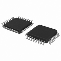
C8051F930-GQ Silicon Laboratories Inc, C8051F930-GQ Datasheet - Page 117

C8051F930-GQ
Manufacturer Part Number
C8051F930-GQ
Description
IC 8051 MCU 64K FLASH 32-LQFP
Manufacturer
Silicon Laboratories Inc
Series
C8051F9xxr
Specifications of C8051F930-GQ
Program Memory Type
FLASH
Program Memory Size
64KB (64K x 8)
Package / Case
32-LQFP
Core Processor
8051
Core Size
8-Bit
Speed
25MHz
Connectivity
SMBus (2-Wire/I²C), SPI, UART/USART
Peripherals
Brown-out Detect/Reset, POR, PWM, Temp Sensor, WDT
Number Of I /o
24
Ram Size
4.25K x 8
Voltage - Supply (vcc/vdd)
0.9 V ~ 3.6 V
Data Converters
A/D 23x10b
Oscillator Type
Internal
Operating Temperature
-40°C ~ 85°C
Processor Series
C8051F9x
Core
8051
Data Bus Width
8 bit
Data Ram Size
4.25 KB
Interface Type
I2C/SMBus/SPI/UART
Maximum Clock Frequency
25 MHz
Number Of Programmable I/os
24
Number Of Timers
4
Operating Supply Voltage
0.9 V to 3.6 V
Maximum Operating Temperature
+ 85 C
Mounting Style
SMD/SMT
3rd Party Development Tools
PK51, CA51, A51, ULINK2
Development Tools By Supplier
C8051F930DK
Minimum Operating Temperature
- 40 C
On-chip Adc
23-ch x 10-bit
No. Of I/o's
24
Ram Memory Size
4KB
Cpu Speed
25MHz
No. Of Timers
4
Rohs Compliant
Yes
Lead Free Status / RoHS Status
Lead free / RoHS Compliant
For Use With
336-1478 - PLATFORM PROG TOOLSTCK F920,F930336-1477 - PLATFORM PROG TOOLSTCK F920,F930336-1473 - KIT DEV C8051F920,F921,F930,F931336-1472 - BOARD TARGET/PROTO W/C8051F930
Eeprom Size
-
Lead Free Status / Rohs Status
Lead free / RoHS Compliant
Other names
336-1466
Available stocks
Company
Part Number
Manufacturer
Quantity
Price
Company:
Part Number:
C8051F930-GQ
Manufacturer:
SILICON
Quantity:
3 500
Company:
Part Number:
C8051F930-GQ
Manufacturer:
Silicon Laboratories Inc
Quantity:
10 000
Company:
Part Number:
C8051F930-GQR
Manufacturer:
Silicon Laboratories Inc
Quantity:
10 000
Part Number:
C8051F930-GQR
Manufacturer:
SILICON LABS/èٹ¯ç§‘
Quantity:
20 000
- Current page: 117 of 324
- Download datasheet (3Mb)
10.5. External Memory Interface Operating Modes
The external data memory space can be configured in one of four operating modes, shown in Figure 10.3,
based on the EMIF Mode bits in the EMI0CF register (SFR Definition 10.2). These modes are summarized
below. Timing diagrams for the different modes can be found in Section “10.6. External Memory Interface
Timing” on page 118.
10.5.1. Internal XRAM Only
When EMI0CF.[3:2] are set to 00, all MOVX instructions will target the internal XRAM space on the device.
Memory accesses to addresses beyond the populated space will wrap, and will always target on-chip
XRAM. As an example, if the entire address space is consecutively written and the data pointer is
incremented after each write, the write pointer will always point to the first byte of on-chip XRAM after the
last byte of on-chip XRAM has been written.
•
•
10.5.2. Split Mode without Bank Select
When EMI0CF.[3:2] are set to 01, the XRAM memory map is split into two areas, on-chip space and off-
chip space.
•
•
•
•
EMI0CF[3:2] = 00
On-Chip XRAM
On-Chip XRAM
On-Chip XRAM
On-Chip XRAM
On-Chip XRAM
On-Chip XRAM
8-bit MOVX operations use the contents of EMI0CN to determine the high-byte of the effective address
and R0 or R1 to determine the low-byte of the effective address.
16-bit MOVX operations use the contents of the 16-bit DPTR to determine the effective address.
Effective addresses below the on-chip XRAM boundary will access on-chip XRAM space.
Effective addresses above the on-chip XRAM boundary will access off-chip space.
8-bit MOVX operations use the contents of EMI0CN to determine whether the memory access is on-
chip or off-chip. However, in the “No Bank Select” mode, an 8-bit MOVX operation will not drive the
upper 4-bits A[11:8] of the Address Bus during an off-chip access. This allows the user to manip-
ulate the upper address bits at will by setting the Port state directly via the port latches. This behavior
is in contrast with “Split Mode with Bank Select” described below. The lower 8-bits of the Address Bus
A[7:0] are driven, determined by R0 or R1.
16-bit MOVX operations use the contents of DPTR to determine whether the memory access is on-
chip or off-chip, and unlike 8-bit MOVX operations, the full 12-bits of the Address Bus A[11:0] are
driven during the off-chip transaction.
0xFFFF
0x0000
EMI0CF[3:2] = 01
(No Bank Select)
On-Chip XRAM
Off-Chip
Memory
Figure 10.3. EMIF Operating Modes
0xFFFF
0x0000
Rev. 1.1
EMI0CF[3:2] = 10
On-Chip XRAM
(Bank Select)
C8051F93x-C8051F92x
Off-Chip
Memory
0xFFFF
0x0000
EMI0CF[3:2] = 11
Off-Chip
Memory
0xFFFF
0x0000
117
Related parts for C8051F930-GQ
Image
Part Number
Description
Manufacturer
Datasheet
Request
R
Part Number:
Description:
SMD/C°/SINGLE-ENDED OUTPUT SILICON OSCILLATOR
Manufacturer:
Silicon Laboratories Inc
Part Number:
Description:
Manufacturer:
Silicon Laboratories Inc
Datasheet:
Part Number:
Description:
N/A N/A/SI4010 AES KEYFOB DEMO WITH LCD RX
Manufacturer:
Silicon Laboratories Inc
Datasheet:
Part Number:
Description:
N/A N/A/SI4010 SIMPLIFIED KEY FOB DEMO WITH LED RX
Manufacturer:
Silicon Laboratories Inc
Datasheet:
Part Number:
Description:
N/A/-40 TO 85 OC/EZLINK MODULE; F930/4432 HIGH BAND (REV E/B1)
Manufacturer:
Silicon Laboratories Inc
Part Number:
Description:
EZLink Module; F930/4432 Low Band (rev e/B1)
Manufacturer:
Silicon Laboratories Inc
Part Number:
Description:
I°/4460 10 DBM RADIO TEST CARD 434 MHZ
Manufacturer:
Silicon Laboratories Inc
Part Number:
Description:
I°/4461 14 DBM RADIO TEST CARD 868 MHZ
Manufacturer:
Silicon Laboratories Inc
Part Number:
Description:
I°/4463 20 DBM RFSWITCH RADIO TEST CARD 460 MHZ
Manufacturer:
Silicon Laboratories Inc
Part Number:
Description:
I°/4463 20 DBM RADIO TEST CARD 868 MHZ
Manufacturer:
Silicon Laboratories Inc
Part Number:
Description:
I°/4463 27 DBM RADIO TEST CARD 868 MHZ
Manufacturer:
Silicon Laboratories Inc
Part Number:
Description:
I°/4463 SKYWORKS 30 DBM RADIO TEST CARD 915 MHZ
Manufacturer:
Silicon Laboratories Inc
Part Number:
Description:
N/A N/A/-40 TO 85 OC/4463 RFMD 30 DBM RADIO TEST CARD 915 MHZ
Manufacturer:
Silicon Laboratories Inc
Part Number:
Description:
I°/4463 20 DBM RADIO TEST CARD 169 MHZ
Manufacturer:
Silicon Laboratories Inc


