C8051F930-GQ Silicon Laboratories Inc, C8051F930-GQ Datasheet - Page 177
C8051F930-GQ
Manufacturer Part Number
C8051F930-GQ
Description
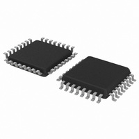
IC 8051 MCU 64K FLASH 32-LQFP
Manufacturer
Silicon Laboratories Inc
Series
C8051F9xxr
Specifications of C8051F930-GQ
Program Memory Type
FLASH
Program Memory Size
64KB (64K x 8)
Package / Case
32-LQFP
Core Processor
8051
Core Size
8-Bit
Speed
25MHz
Connectivity
SMBus (2-Wire/I²C), SPI, UART/USART
Peripherals
Brown-out Detect/Reset, POR, PWM, Temp Sensor, WDT
Number Of I /o
24
Ram Size
4.25K x 8
Voltage - Supply (vcc/vdd)
0.9 V ~ 3.6 V
Data Converters
A/D 23x10b
Oscillator Type
Internal
Operating Temperature
-40°C ~ 85°C
Processor Series
C8051F9x
Core
8051
Data Bus Width
8 bit
Data Ram Size
4.25 KB
Interface Type
I2C/SMBus/SPI/UART
Maximum Clock Frequency
25 MHz
Number Of Programmable I/os
24
Number Of Timers
4
Operating Supply Voltage
0.9 V to 3.6 V
Maximum Operating Temperature
+ 85 C
Mounting Style
SMD/SMT
3rd Party Development Tools
PK51, CA51, A51, ULINK2
Development Tools By Supplier
C8051F930DK
Minimum Operating Temperature
- 40 C
On-chip Adc
23-ch x 10-bit
No. Of I/o's
24
Ram Memory Size
4KB
Cpu Speed
25MHz
No. Of Timers
4
Rohs Compliant
Yes
Lead Free Status / RoHS Status
Lead free / RoHS Compliant
For Use With
336-1478 - PLATFORM PROG TOOLSTCK F920,F930336-1477 - PLATFORM PROG TOOLSTCK F920,F930336-1473 - KIT DEV C8051F920,F921,F930,F931336-1472 - BOARD TARGET/PROTO W/C8051F930
Eeprom Size
-
Lead Free Status / Rohs Status
Lead free / RoHS Compliant
Other names
336-1466
Available stocks
Company
Part Number
Manufacturer
Quantity
Price
Company:

Part Number:
C8051F930-GQ
Manufacturer:
SILICON
Quantity:
3 500
Company:
Part Number:
C8051F930-GQ
Manufacturer:
Silicon Laboratories Inc
Quantity:
10 000
Company:
Part Number:
C8051F930-GQR
Manufacturer:
Silicon Laboratories Inc
Quantity:
10 000
Part Number:
C8051F930-GQR
Manufacturer:
SILICON LABS/èٹ¯ç§‘
Quantity:
20 000


16.9. DC-DC Converter Register Descriptions
The SFRs used to configure the dc-dc converter are described in the following register descriptions. The
reset values for these registers can be used as-is in most systems; therefore, no software intervention or
initialization is required.
SFR Definition 16.1. DC0CN: DC-DC Converter Control
SFR Page = 0x0; SFR Address = 0x97
Reset
Name
Type
7:6
2:0
Bit
Bit
5
4
3
MINPW[1:0] DC
VSEL[2:0]
Reserved
SWSEL
Name
SYNC
7
0
MINPW
R/W
Specifies the minimum pulse width.
00: No minimum duty cycle.
01: Minimum pulse width is 20 ns.
10: Minimum pulse width is 40 ns.
11: Minimum pulse width is 80 ns.
DC-DC Converter Switch Select.
Selects one of two possible converter switch sizes to maximize efficiency.
0: The large switches are selected (best efficiency for high output currents).
1: The small switches are selected (best efficiency for low output currents).
Reserved. Always Write to 0.
ADC0 Synchronization Enable.
When synchronization is enabled, the ADC0SC[4:0] bits in the ADC0CF register
must be set to 00000b. Behavior as described is valid in REVC and later devices.
0: The ADC is not synchronized to the dc-dc converter.
1: The ADC is synchronized to the dc-dc converter. ADC0 tracking is performed
during the longest quiet time of the dc-dc converter switching cycle and ADC0 SAR
clock is also synchronized to the dc-dc converter switching cycle.
DC
Specifies the target output voltage.
000: Target output voltage is 1.8 V.
001: Target output voltage is 1.9 V.
010: Target output voltage is 2.0 V.
011: Target output voltage is 2.1 V.
100: Target output voltage is 2.4 V.
101: Target output voltage is 2.7 V.
110: Target output voltage is 3.0 V.
111: Target output voltage is 3.3 V.
0
6
-
-
DC Converter Minimum Pulse Width.
DC Converter Output Voltage Select.
SWSEL
R/W
5
1
Reserved
R/W
Rev. 1.1
4
0
C8051F93x-C8051F92x
Function
SYNC
R/W
3
0
2
0
VSEL
R/W
1
0
0
1
177
Related parts for C8051F930-GQ
Image
Part Number
Description
Manufacturer
Datasheet
Request
R

Part Number:
Description:
SMD/C°/SINGLE-ENDED OUTPUT SILICON OSCILLATOR
Manufacturer:
Silicon Laboratories Inc
Part Number:
Description:
Manufacturer:
Silicon Laboratories Inc
Datasheet:
Part Number:
Description:
N/A N/A/SI4010 AES KEYFOB DEMO WITH LCD RX
Manufacturer:
Silicon Laboratories Inc
Datasheet:
Part Number:
Description:
N/A N/A/SI4010 SIMPLIFIED KEY FOB DEMO WITH LED RX
Manufacturer:
Silicon Laboratories Inc
Datasheet:
Part Number:
Description:
N/A/-40 TO 85 OC/EZLINK MODULE; F930/4432 HIGH BAND (REV E/B1)
Manufacturer:
Silicon Laboratories Inc
Part Number:
Description:
EZLink Module; F930/4432 Low Band (rev e/B1)
Manufacturer:
Silicon Laboratories Inc
Part Number:
Description:
I°/4460 10 DBM RADIO TEST CARD 434 MHZ
Manufacturer:
Silicon Laboratories Inc
Part Number:
Description:
I°/4461 14 DBM RADIO TEST CARD 868 MHZ
Manufacturer:
Silicon Laboratories Inc
Part Number:
Description:
I°/4463 20 DBM RFSWITCH RADIO TEST CARD 460 MHZ
Manufacturer:
Silicon Laboratories Inc
Part Number:
Description:
I°/4463 20 DBM RADIO TEST CARD 868 MHZ
Manufacturer:
Silicon Laboratories Inc
Part Number:
Description:
I°/4463 27 DBM RADIO TEST CARD 868 MHZ
Manufacturer:
Silicon Laboratories Inc
Part Number:
Description:
I°/4463 SKYWORKS 30 DBM RADIO TEST CARD 915 MHZ
Manufacturer:
Silicon Laboratories Inc
Part Number:
Description:
N/A N/A/-40 TO 85 OC/4463 RFMD 30 DBM RADIO TEST CARD 915 MHZ
Manufacturer:
Silicon Laboratories Inc
Part Number:
Description:
I°/4463 20 DBM RADIO TEST CARD 169 MHZ
Manufacturer:
Silicon Laboratories Inc