C8051F930-GQ Silicon Laboratories Inc, C8051F930-GQ Datasheet - Page 4
C8051F930-GQ
Manufacturer Part Number
C8051F930-GQ
Description
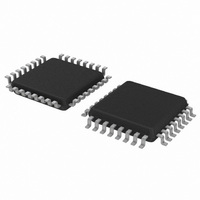
IC 8051 MCU 64K FLASH 32-LQFP
Manufacturer
Silicon Laboratories Inc
Series
C8051F9xxr
Specifications of C8051F930-GQ
Program Memory Type
FLASH
Program Memory Size
64KB (64K x 8)
Package / Case
32-LQFP
Core Processor
8051
Core Size
8-Bit
Speed
25MHz
Connectivity
SMBus (2-Wire/I²C), SPI, UART/USART
Peripherals
Brown-out Detect/Reset, POR, PWM, Temp Sensor, WDT
Number Of I /o
24
Ram Size
4.25K x 8
Voltage - Supply (vcc/vdd)
0.9 V ~ 3.6 V
Data Converters
A/D 23x10b
Oscillator Type
Internal
Operating Temperature
-40°C ~ 85°C
Processor Series
C8051F9x
Core
8051
Data Bus Width
8 bit
Data Ram Size
4.25 KB
Interface Type
I2C/SMBus/SPI/UART
Maximum Clock Frequency
25 MHz
Number Of Programmable I/os
24
Number Of Timers
4
Operating Supply Voltage
0.9 V to 3.6 V
Maximum Operating Temperature
+ 85 C
Mounting Style
SMD/SMT
3rd Party Development Tools
PK51, CA51, A51, ULINK2
Development Tools By Supplier
C8051F930DK
Minimum Operating Temperature
- 40 C
On-chip Adc
23-ch x 10-bit
No. Of I/o's
24
Ram Memory Size
4KB
Cpu Speed
25MHz
No. Of Timers
4
Rohs Compliant
Yes
Lead Free Status / RoHS Status
Lead free / RoHS Compliant
For Use With
336-1478 - PLATFORM PROG TOOLSTCK F920,F930336-1477 - PLATFORM PROG TOOLSTCK F920,F930336-1473 - KIT DEV C8051F920,F921,F930,F931336-1472 - BOARD TARGET/PROTO W/C8051F930
Eeprom Size
-
Lead Free Status / Rohs Status
Lead free / RoHS Compliant
Other names
336-1466
Available stocks
Company
Part Number
Manufacturer
Quantity
Price
Company:

Part Number:
C8051F930-GQ
Manufacturer:
SILICON
Quantity:
3 500
Company:
Part Number:
C8051F930-GQ
Manufacturer:
Silicon Laboratories Inc
Quantity:
10 000
Company:
Part Number:
C8051F930-GQR
Manufacturer:
Silicon Laboratories Inc
Quantity:
10 000
Part Number:
C8051F930-GQR
Manufacturer:
SILICON LABS/èٹ¯ç§‘
Quantity:
20 000


C8051F93x-C8051F92x
8. CIP-51 Microcontroller ......................................................................................... 100
9. Memory Organization........................................................................................... 109
10. External Data Memory Interface and On-Chip XRAM........................................ 113
11. Special Function Registers ................................................................................. 126
12. Interrupt Handler .................................................................................................. 133
13. Flash Memory ....................................................................................................... 145
4
7.2. Comparator Outputs ......................................................................................... 91
7.3. Comparator Response Time............................................................................. 92
7.4. Comparator Hysterisis ...................................................................................... 92
7.5. Comparator Register Descriptions.................................................................... 93
7.6. Comparator0 and Comparator1 Analog Multiplexers........................................ 97
8.1. Instruction Set ................................................................................................. 101
8.2. CIP-51 Register Descriptions.......................................................................... 106
9.1. Program Memory ............................................................................................ 110
9.2. Data Memory .................................................................................................. 111
10.1.Accessing XRAM............................................................................................ 113
10.2.Configuring the External Memory Interface for Off-Chip Access.................... 114
10.3.External Memory Interface Port Input/Output Configuration........................... 114
10.4.Multiplexed External Memory Interface .......................................................... 115
10.5.External Memory Interface Operating Modes................................................. 117
10.6.External Memory Interface Timing.................................................................. 118
10.7.EMIF Special Function Registers ................................................................... 119
10.8.EMIF Timing Diagrams................................................................................... 122
11.1.SFR Paging .................................................................................................... 127
12.1.Enabling Interrupt Sources ............................................................................. 133
12.2.MCU Interrupt Sources and Vectors............................................................... 133
12.3.Interrupt Priorities ........................................................................................... 134
12.4.Interrupt Latency............................................................................................. 134
12.5.Interrupt Register Descriptions ....................................................................... 136
12.6.External Interrupts INT0 and INT1.................................................................. 143
13.1.Programming The Flash Memory ................................................................... 145
8.1.1. Instruction and CPU Timing ................................................................... 101
9.1.1. MOVX Instruction and Program Memory ............................................... 110
9.2.1. Internal RAM .......................................................................................... 111
9.2.2. External RAM ......................................................................................... 112
10.1.1.16-Bit MOVX Example ........................................................................... 113
10.1.2.8-Bit MOVX Example ............................................................................. 113
10.5.1.Internal XRAM Only ............................................................................... 117
10.5.2.Split Mode without Bank Select.............................................................. 117
10.5.3.Split Mode with Bank Select................................................................... 118
10.5.4.External Only.......................................................................................... 118
10.8.1.Multiplexed 16-bit MOVX: EMI0CF[3:2] = 01, 10, or 11......................... 122
10.8.2.Multiplexed 8-bit MOVX without Bank Select: EMI0CF[3:2] = 01 or 11. 123
13.1.1.Flash Lock and Key Functions ............................................................... 145
13.1.2.Flash Erase Procedure .......................................................................... 146
Rev. 1.1
Related parts for C8051F930-GQ
Image
Part Number
Description
Manufacturer
Datasheet
Request
R

Part Number:
Description:
SMD/C°/SINGLE-ENDED OUTPUT SILICON OSCILLATOR
Manufacturer:
Silicon Laboratories Inc
Part Number:
Description:
Manufacturer:
Silicon Laboratories Inc
Datasheet:
Part Number:
Description:
N/A N/A/SI4010 AES KEYFOB DEMO WITH LCD RX
Manufacturer:
Silicon Laboratories Inc
Datasheet:
Part Number:
Description:
N/A N/A/SI4010 SIMPLIFIED KEY FOB DEMO WITH LED RX
Manufacturer:
Silicon Laboratories Inc
Datasheet:
Part Number:
Description:
N/A/-40 TO 85 OC/EZLINK MODULE; F930/4432 HIGH BAND (REV E/B1)
Manufacturer:
Silicon Laboratories Inc
Part Number:
Description:
EZLink Module; F930/4432 Low Band (rev e/B1)
Manufacturer:
Silicon Laboratories Inc
Part Number:
Description:
I°/4460 10 DBM RADIO TEST CARD 434 MHZ
Manufacturer:
Silicon Laboratories Inc
Part Number:
Description:
I°/4461 14 DBM RADIO TEST CARD 868 MHZ
Manufacturer:
Silicon Laboratories Inc
Part Number:
Description:
I°/4463 20 DBM RFSWITCH RADIO TEST CARD 460 MHZ
Manufacturer:
Silicon Laboratories Inc
Part Number:
Description:
I°/4463 20 DBM RADIO TEST CARD 868 MHZ
Manufacturer:
Silicon Laboratories Inc
Part Number:
Description:
I°/4463 27 DBM RADIO TEST CARD 868 MHZ
Manufacturer:
Silicon Laboratories Inc
Part Number:
Description:
I°/4463 SKYWORKS 30 DBM RADIO TEST CARD 915 MHZ
Manufacturer:
Silicon Laboratories Inc
Part Number:
Description:
N/A N/A/-40 TO 85 OC/4463 RFMD 30 DBM RADIO TEST CARD 915 MHZ
Manufacturer:
Silicon Laboratories Inc
Part Number:
Description:
I°/4463 20 DBM RADIO TEST CARD 169 MHZ
Manufacturer:
Silicon Laboratories Inc