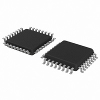
C8051F930-GQ Silicon Laboratories Inc, C8051F930-GQ Datasheet - Page 67

C8051F930-GQ
Manufacturer Part Number
C8051F930-GQ
Description
IC 8051 MCU 64K FLASH 32-LQFP
Manufacturer
Silicon Laboratories Inc
Series
C8051F9xxr
Specifications of C8051F930-GQ
Program Memory Type
FLASH
Program Memory Size
64KB (64K x 8)
Package / Case
32-LQFP
Core Processor
8051
Core Size
8-Bit
Speed
25MHz
Connectivity
SMBus (2-Wire/I²C), SPI, UART/USART
Peripherals
Brown-out Detect/Reset, POR, PWM, Temp Sensor, WDT
Number Of I /o
24
Ram Size
4.25K x 8
Voltage - Supply (vcc/vdd)
0.9 V ~ 3.6 V
Data Converters
A/D 23x10b
Oscillator Type
Internal
Operating Temperature
-40°C ~ 85°C
Processor Series
C8051F9x
Core
8051
Data Bus Width
8 bit
Data Ram Size
4.25 KB
Interface Type
I2C/SMBus/SPI/UART
Maximum Clock Frequency
25 MHz
Number Of Programmable I/os
24
Number Of Timers
4
Operating Supply Voltage
0.9 V to 3.6 V
Maximum Operating Temperature
+ 85 C
Mounting Style
SMD/SMT
3rd Party Development Tools
PK51, CA51, A51, ULINK2
Development Tools By Supplier
C8051F930DK
Minimum Operating Temperature
- 40 C
On-chip Adc
23-ch x 10-bit
No. Of I/o's
24
Ram Memory Size
4KB
Cpu Speed
25MHz
No. Of Timers
4
Rohs Compliant
Yes
Lead Free Status / RoHS Status
Lead free / RoHS Compliant
For Use With
336-1478 - PLATFORM PROG TOOLSTCK F920,F930336-1477 - PLATFORM PROG TOOLSTCK F920,F930336-1473 - KIT DEV C8051F920,F921,F930,F931336-1472 - BOARD TARGET/PROTO W/C8051F930
Eeprom Size
-
Lead Free Status / Rohs Status
Lead free / RoHS Compliant
Other names
336-1466
Available stocks
Company
Part Number
Manufacturer
Quantity
Price
Company:
Part Number:
C8051F930-GQ
Manufacturer:
SILICON
Quantity:
3 500
Company:
Part Number:
C8051F930-GQ
Manufacturer:
Silicon Laboratories Inc
Quantity:
10 000
Company:
Part Number:
C8051F930-GQR
Manufacturer:
Silicon Laboratories Inc
Quantity:
10 000
Part Number:
C8051F930-GQR
Manufacturer:
SILICON LABS/èٹ¯ç§‘
Quantity:
20 000
5.2.
ADC0 has a maximum conversion speed of 300 ksps. The ADC0 conversion clock (SARCLK) is a divided
version of the system clock when Burst Mode is disabled (BURSTEN = 0), or a divided version of the low
power oscillator when Burst Mode is enabled (BURSEN = 1). The clock divide value is determined by the
AD0SC bits in the ADC0CF register.
5.2.1. Starting a Conversion
A conversion can be initiated in one of five ways, depending on the programmed states of the ADC0 Start
of Conversion Mode bits (AD0CM2–0) in register ADC0CN. Conversions may be initiated by one of the fol-
lowing:
Writing a 1 to AD0BUSY provides software control of ADC0 whereby conversions are performed "on-
demand". During conversion, the AD0BUSY bit is set to logic 1 and reset to logic 0 when the conversion is
complete. The falling edge of AD0BUSY triggers an interrupt (when enabled) and sets the ADC0 interrupt
flag (AD0INT). When polling for ADC conversion completions, the ADC0 interrupt flag (AD0INT) should be
used. Converted data is available in the ADC0 data registers, ADC0H:ADC0L, when bit AD0INT is logic 1.
When Timer 2 or Timer 3 overflows are used as the conversion source, Low Byte overflows are used if
Timer 2/3 is in 8-bit mode; High byte overflows are used if Timer 2/3 is in 16-bit mode. See “25. Timers” on
page 278 for timer configuration.
Important Note About Using CNVSTR: The CNVSTR input pin also functions as Port pin P0.6. When the
CNVSTR input is used as the ADC0 conversion source, Port pin P0.6 should be skipped by the Digital
Crossbar. To configure the Crossbar to skip P0.6, set to 1 Bit 6 in register P0SKIP. See “21. Port Input/Out-
put” on page 212 for details on Port I/O configuration.
Important Note: When operating the device in one-cell mode, there is an option available to automatically
synchronize the start of conversion with the quietest portion of the dc-dc converter switching cycle. Activat-
ing this option may help to reduce interference from internal or external power supply noise generated by
the dc-dc converter. Asserting this bit will hold off the start of an ADC conversion initiated by any of the
methods described above until the ADC receives a synchronizing signal from the dc-dc converter. The
delay in initiation of the conversion can be as much as one cycle of the dc-dc converter clock, which is
625 ns at the minimum dc-dc clock frequency of 1.6 MHz. For rev C and later C8051F93x-92x devices, the
synchronization feature also causes the dc-dc converter clock to be used as the ADC0 conversion clock.
The maximum conversion rate will be limited to approximately 170 ksps at the maximum dc-dc converter
clock rate of 3.2 MHz. In this mode, the ADC0 SAR Conversion Clock Divider must be set to 1 by setting
AD0SC[4:0] = 00000b in SFR register ADC0CF. To provide additional flexibility in minimizing noise, the
ADC0 conversion clock provided by the dc-dc converter can be inverted by setting the AD0CKINV bit in the
DC0CF register. For additional information on the synchronization feature, see the description of the SYNC
bit in “SFR Definition 16.1. DC0CN: DC-DC Converter Control” on page 177 and the description of the
AD0CKINV bit in “SFR Definition 16.2. DC0CF: DC-DC Converter Configuration” on page 178. This bit
must be set to 0 in two-cell mode for the ADC to operate.
Modes of Operation
1. Writing a 1 to the AD0BUSY bit of register ADC0CN
2. A Timer 0 overflow (i.e., timed continuous conversions)
3. A Timer 2 overflow
4. A Timer 3 overflow
5. A rising edge on the CNVSTR input signal (pin P0.6)
Rev. 1.1
C8051F93x-C8051F92x
67


