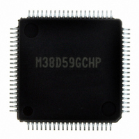
M38D59GCHP#U0 Renesas Electronics America, M38D59GCHP#U0 Datasheet - Page 129

M38D59GCHP#U0
Manufacturer Part Number
M38D59GCHP#U0
Description
IC 740/38D5 MCU QZ-ROM 80LQFP
Manufacturer
Renesas Electronics America
Series
740/38000r
Datasheet
1.M38D58G8FPU0.pdf
(144 pages)
Specifications of M38D59GCHP#U0
Core Processor
740
Core Size
8-Bit
Speed
12.5MHz
Connectivity
SIO, UART/USART
Peripherals
LCD, LED, PWM, WDT
Number Of I /o
59
Program Memory Size
48KB (48K x 8)
Program Memory Type
QzROM
Ram Size
2K x 8
Voltage - Supply (vcc/vdd)
1.8 V ~ 5.5 V
Data Converters
A/D 8x10b
Oscillator Type
Internal
Operating Temperature
-20°C ~ 85°C
Package / Case
80-LQFP
Lead Free Status / RoHS Status
Lead free / RoHS Compliant
Eeprom Size
-
Available stocks
Company
Part Number
Manufacturer
Quantity
Price
38D5 Group
Rev.3.04
REJ03B0158-0304
10. Write to Timer X
(1) Timer X can select either writing data to both the latch and
(2) Switch the frequency division or count source* while the
*This also applies when the frequency divider output is selected
11. Setting Timer X Mode Register
When PWM mode or IGBT output mode is set, be sure to set the
write control bit in the timer X mode register to “1” (writing to
latch only). After writing to the timer X register (high-order), the
contents of both registers are simultaneously reflected in the
output waveform at the next underflow.
12. Timer X Output Control Functions
To use the output control functions (INT
levels of INT
“L” for the rising edge active before switching to IGBT output
mode.
13. CNTR
(1) Setting the CNTR
(2) When the pulse width is measured, set bit 7 of the CNTR
14. When Timer X Pulse Width Measurement Mode
When timer X pulse mode measurement mode is used, enable the
event counter wind control data (bit 5 of timer X mode register
(address 002D
<Reason>
If the event counter window control data (bit 5 of timer X mode
r egister (address 002 D
enable/disable the CNTR
the timer 1 underflow.
as the timer count source and the count source is switched in
conjunction with a transition between operating modes (on-
chip oscillator mode, X
careful when changing settings in the CPU mode register.
Used
the timer at the same time or writing data only by the timer
X write control bit (b3) in the timer X mode register
(address 002D
is written to the timer X address, the value is set into the
reload latch and the timer is updated at the next underflow.
After a reset release, if a value is written to the timer X
address, the value is set into the timer and the timer latch at
the same time, because they are written simultaneously.
When writing to the latch only, if the write timing to the
high-order reload latch and the underflow timing are almost
the same, the value is set into the timer and the timer latch at
the same time. At this time, count is stopped during write
operation to the high-order reload latch.
timer count is stopped.
interrupt active edge at the same time.
active edge switch bits to “0”.
0
Active Edge Selection
1
May 20, 2008 Page 127 of 134
16
and INT
)) by setting to “0”.
16
). When writing to the latch only, if a value
0
2
active edge switch bits also affects the
to “H” for the falling edge active or to
0
IN
input, the input is not accepted after
1 6
)) is set to “1” (disabled) to
mode, or low-speed mode). Be
1
and INT
2
), set the
0
15. CNTR1 Active Edge Selection
Setting the CNTR
interrupt active edge at the same time.
However, in pulse width HL continuous HL measurement mode,
the CNTR
falling edges of the pin regardless of the settings of the CNTR
active edge switch bits.
16. Read from/Write to Timer Y
(1) When reading from/writing to timer Y, read from/write to
(2) Timer Y can select either writing data to both the latch and
(3) Switch the frequency division or count source* while the
*This also applies when the frequency divider output is selected
as the timer count source and the count source is switched in
conjunction with a transition between operating modes (on-
chip oscillator mode, X
careful when changing settings in the CPU mode register.
both the high-order and low-order bytes of timer Y. To read
the value, read the high-order bytes first and the low-order
bytes next. To write the value, write the low-order bytes first
and the high-order bytes next.
Writing/reading should be preformed in 16-bit units. If
write/read operation is changed in progress, normal
operation will not be performed.
the timer at the same time or writing data only by the timer
Y write control bit (b0) in the timer Y control register
(address 0039
is written to the timer Y address, the value is set into the
reload latch and the timer is updated at the next underflow.
After a reset release, if a value is written to the timer Y
address, the value is set into the timer and the timer latch at
the same time, because they are written simultaneously.
When writing to the latch only, if the write timing to the
high-order reload latch and the underflow timing are almost
the same, the value is set into the timer and the timer latch at
the same time. At this time, count is stopped during write
operation to the high-order reload latch.
timer count is stopped.
1
interrupt request is generated at both rising and
16
1
). When writing to the latch only, if a value
active edge switch bits also affects the
IN
mode, or low-speed mode). Be
1


