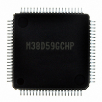
M38D59GCHP#U0 Renesas Electronics America, M38D59GCHP#U0 Datasheet - Page 66

M38D59GCHP#U0
Manufacturer Part Number
M38D59GCHP#U0
Description
IC 740/38D5 MCU QZ-ROM 80LQFP
Manufacturer
Renesas Electronics America
Series
740/38000r
Datasheet
1.M38D58G8FPU0.pdf
(144 pages)
Specifications of M38D59GCHP#U0
Core Processor
740
Core Size
8-Bit
Speed
12.5MHz
Connectivity
SIO, UART/USART
Peripherals
LCD, LED, PWM, WDT
Number Of I /o
59
Program Memory Size
48KB (48K x 8)
Program Memory Type
QzROM
Ram Size
2K x 8
Voltage - Supply (vcc/vdd)
1.8 V ~ 5.5 V
Data Converters
A/D 8x10b
Oscillator Type
Internal
Operating Temperature
-20°C ~ 85°C
Package / Case
80-LQFP
Lead Free Status / RoHS Status
Lead free / RoHS Compliant
Eeprom Size
-
Available stocks
Company
Part Number
Manufacturer
Quantity
Price
38D5 Group
Rev.3.04
REJ03B0158-0304
• Oscillation Control
(1) Stop Mode
If the STP instruction is executed, the system clock φ stops at an
“H” level, and main clock and sub-clock oscillators stop.
In this time, values set previously to timer 1 latch and timer 2 latch
are loaded automatically to timer 1 and timer 2. Set the values * to
generate the wait time required for oscillation stabilization to
timer 1 latch and timer 2 latch (low-order 8 bits of timer 1 and
high-order 8 bits of timer 2) before the STP instruction.
The frequency divider for timer 1 is used for the timer 1 count
source, and the output of timer 1 is forcibly connected to timer 2. In
this time, bits 0 to 5 of the timer 12 mode register are cleared to “0”.
The values of the timer 12 frequency divider selection register
are not changed.
Set the interrupt enable bits of the timer 1 and timer 2 to be
disabled (“0”) before executing the STP instruction.
*: Reference (Set values according to your oscillator and system.)
version:
When an external interrupt is received, the clock set according to
the OSCSEL pin state starts oscillating in the QzROM version.
The operation mode at returning is decided by the clock that set
according to the OSCSEL pin state.
Bits 3, 5, 6, and 7 of CPUM and bit 0 of CPUM2 are forcibly
changed by the OSCSEL pin state. In the flash memory version,
the on-chip oscillator starts oscillating and the operation mode at
returning is set to on-chip oscillator mode. The bit 3 of CPUM is
changed to “0”, bits 5, 6 and 7 of CPUM are changed to “1”, and
the bit 0 of CPUM2 is changed to “0” forcibly.
Oscillator restarts when reset occurs or an interrupt request is
received, but the system clock φ is not supplied to the CPU until
timer 2 underflows. This allows time for the clock circuit
oscillation to stabilize.
(2) Wait Mode
If the WIT instruction is executed, only the system clock φ stops
at an “H” state. The states of main clock, on-chip oscillator and
sub clock are the same as the state before executing the WIT
instruction, and oscillation does not stop. Since supply of system
clock φ is started immediately after the interrupt is received, the
instruction can be executed immediately.
OSCSEL = “L” of the QzROM version and flash memory
OSCSEL = “H” of the QzROM version:
.......................................................................... 0005
..........................................................................01FF
May 20, 2008 Page 64 of 134
16
16
or more
or more
Fig. 60 Ceramic resonator circuit example
Fig. 61 External clock input circuit
Note : Insert a damping resistor if required.
The resistance will vary depending on the oscillator and the oscillation drive
capacity setting.
Use the value recommended by the maker of the oscillator.
Also, if the oscillator manufacturer's data sheet specifies that a feedback
resistor be added external to the chip though a feedback resistor exists on-chip,
insert a feedback resistor between X
X
CIN
X
C
CIN
Rf
CIN
C
Rf
X
CIN
COUT
X
Rd
C
COUT
COUT
External oscillation circuit
Rd
C
COUT
X
V
V
IN
CC
SS
IN
and X
X
X
Open
IN
OUT
C
OUT
IN
X
following the instruction.
OUT
Rd
C
OUT


