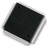
MC912D60CCPVE Freescale Semiconductor, MC912D60CCPVE Datasheet - Page 100

MC912D60CCPVE
Manufacturer Part Number
MC912D60CCPVE
Description
IC MCU 16BIT 112-LQFP
Manufacturer
Freescale Semiconductor
Series
HC12r
Datasheet
1.MC912D60ACFUE8.pdf
(460 pages)
Specifications of MC912D60CCPVE
Core Processor
CPU12
Core Size
16-Bit
Speed
8MHz
Connectivity
CAN, MI Bus, SCI, SPI
Peripherals
POR, PWM, WDT
Number Of I /o
68
Program Memory Size
60KB (60K x 8)
Program Memory Type
FLASH
Eeprom Size
1K x 8
Ram Size
2K x 8
Voltage - Supply (vcc/vdd)
4.5 V ~ 5.5 V
Data Converters
A/D 16x8/10b
Oscillator Type
Internal
Operating Temperature
-40°C ~ 85°C
Package / Case
112-LQFP
Processor Series
HC912D
Core
HC12
Data Bus Width
16 bit
Data Ram Size
2 KB
Interface Type
CAN, SCI, SPI
Maximum Clock Frequency
8 MHz
Number Of Programmable I/os
86
Maximum Operating Temperature
+ 85 C
Mounting Style
SMD/SMT
3rd Party Development Tools
EWHCS12
Minimum Operating Temperature
- 40 C
On-chip Adc
10 bit, 8 Channel
Lead Free Status / RoHS Status
Lead free / RoHS Compliant
Available stocks
Company
Part Number
Manufacturer
Quantity
Price
Company:
Part Number:
MC912D60CCPVE
Manufacturer:
FREESCAL
Quantity:
203
Company:
Part Number:
MC912D60CCPVE
Manufacturer:
Freescale Semiconductor
Quantity:
10 000
- Current page: 100 of 460
- Download datasheet (5Mb)
Flash Memory
7.7 Operation
7.7.1 Bootstrap Operation Single-Chip Mode
Technical Data
100
FEESWAI — Flash EEPROM Stop in Wait Control
HVEN — High-Voltage Enable
ERAS — Erase Control
PGM — Program Control
The Flash EEPROM can contain program and data. On reset, it can
operate as a bootstrap memory to provide the CPU with internal
initialization information during the reset sequence.
After reset, the CPU controlling the system will begin booting up by
fetching the first program address from address $FFFE.
This bit enables the charge pump to supply high voltages for program
and erase operations in the array. HVEN can only be set if either PGM
or ERAS are set and the proper sequence for program or erase is
followed.
This bit configures the memory for erase operation. ERAS is
interlocked with the PGM bit such that both bits cannot be equal to 1
or set to1 at the same time.
This bit configures the memory for program operation. PGM is
interlocked with the ERAS bit such that both bits cannot be equal to 1
or set to1 at the same time.
0 = Do not halt Flash EEPROM clock when the part is in wait mode.
0 = Halt Flash EEPROM clock when the part is in wait mode.
0 = Disables high voltage to array and charge pump off
1 = Enables high voltage to array and charge pump on
0 = Erase operation is not selected.
1 = Erase operation selected.
0 = Program operation is not selected.
1 = Program operation selected.
Flash Memory
MC68HC912D60A — Rev. 3.1
Freescale Semiconductor
Related parts for MC912D60CCPVE
Image
Part Number
Description
Manufacturer
Datasheet
Request
R
Part Number:
Description:
Manufacturer:
Freescale Semiconductor, Inc
Datasheet:
Part Number:
Description:
Manufacturer:
Freescale Semiconductor, Inc
Datasheet:
Part Number:
Description:
Manufacturer:
Freescale Semiconductor, Inc
Datasheet:
Part Number:
Description:
Manufacturer:
Freescale Semiconductor, Inc
Datasheet:
Part Number:
Description:
Manufacturer:
Freescale Semiconductor, Inc
Datasheet:
Part Number:
Description:
Manufacturer:
Freescale Semiconductor, Inc
Datasheet:
Part Number:
Description:
Manufacturer:
Freescale Semiconductor, Inc
Datasheet:
Part Number:
Description:
Manufacturer:
Freescale Semiconductor, Inc
Datasheet:
Part Number:
Description:
Manufacturer:
Freescale Semiconductor, Inc
Datasheet:
Part Number:
Description:
Manufacturer:
Freescale Semiconductor, Inc
Datasheet:
Part Number:
Description:
Manufacturer:
Freescale Semiconductor, Inc
Datasheet:
Part Number:
Description:
Manufacturer:
Freescale Semiconductor, Inc
Datasheet:
Part Number:
Description:
Manufacturer:
Freescale Semiconductor, Inc
Datasheet:
Part Number:
Description:
Manufacturer:
Freescale Semiconductor, Inc
Datasheet:
Part Number:
Description:
Manufacturer:
Freescale Semiconductor, Inc
Datasheet:


