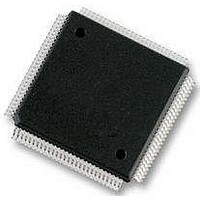
MC912D60CCPVE Freescale Semiconductor, MC912D60CCPVE Datasheet - Page 106

MC912D60CCPVE
Manufacturer Part Number
MC912D60CCPVE
Description
IC MCU 16BIT 112-LQFP
Manufacturer
Freescale Semiconductor
Series
HC12r
Datasheet
1.MC912D60ACFUE8.pdf
(460 pages)
Specifications of MC912D60CCPVE
Core Processor
CPU12
Core Size
16-Bit
Speed
8MHz
Connectivity
CAN, MI Bus, SCI, SPI
Peripherals
POR, PWM, WDT
Number Of I /o
68
Program Memory Size
60KB (60K x 8)
Program Memory Type
FLASH
Eeprom Size
1K x 8
Ram Size
2K x 8
Voltage - Supply (vcc/vdd)
4.5 V ~ 5.5 V
Data Converters
A/D 16x8/10b
Oscillator Type
Internal
Operating Temperature
-40°C ~ 85°C
Package / Case
112-LQFP
Processor Series
HC912D
Core
HC12
Data Bus Width
16 bit
Data Ram Size
2 KB
Interface Type
CAN, SCI, SPI
Maximum Clock Frequency
8 MHz
Number Of Programmable I/os
86
Maximum Operating Temperature
+ 85 C
Mounting Style
SMD/SMT
3rd Party Development Tools
EWHCS12
Minimum Operating Temperature
- 40 C
On-chip Adc
10 bit, 8 Channel
Lead Free Status / RoHS Status
Lead free / RoHS Compliant
Available stocks
Company
Part Number
Manufacturer
Quantity
Price
Company:
Part Number:
MC912D60CCPVE
Manufacturer:
FREESCAL
Quantity:
203
Company:
Part Number:
MC912D60CCPVE
Manufacturer:
Freescale Semiconductor
Quantity:
10 000
- Current page: 106 of 460
- Download datasheet (5Mb)
EEPROM Memory
8.3 EEPROM Selective Write More Zeros
Technical Data
106
program/erase voltage. Programming voltage is derived from the
internal V
The EEPROM can be programmed such that one or multiple bits are
programmed (written to a logic “0”) at a time. However, the user should
never program any bit more than once before erasing the entire byte. In
other words, the user is not allowed to over write a logic “0” with another
“0’.
For some applications it may be advantageous to track more than 10k
events with a single byte of EEPROM by programming one bit at a time.
For that purpose, a special selective bit programming technique is
available. An example is shown here.
Original state of byte = binary 1111:1111 (erased)
First event is recorded by programming bit position 0
Program write = binary 1111:1110;
Second event is recorded by programming bit position 1
Program write = binary 1111:1101;
Third event is recorded by programming bit position 2
Program write = binary 1111:1011;
Fourth event is recorded by programming bit position 3
Program write = binary 1111:0111;
Events five through eight are recorded in a similar fashion.
Note that none of the bit locations are actually programmed more than
once although the byte was programmed eight times.
When this technique is utilized, a program / erase cycle is defined as
multiple writes (up to eight) to a unique location followed by a single
erase sequence.
DD
supply with an internal charge pump.
EEPROM Memory
Result = binary 1111:1110
Result = binary 1111:1100
Result = binary 1111:1000
Result = binary 1111:0000
MC68HC912D60A — Rev. 3.1
Freescale Semiconductor
Related parts for MC912D60CCPVE
Image
Part Number
Description
Manufacturer
Datasheet
Request
R
Part Number:
Description:
Manufacturer:
Freescale Semiconductor, Inc
Datasheet:
Part Number:
Description:
Manufacturer:
Freescale Semiconductor, Inc
Datasheet:
Part Number:
Description:
Manufacturer:
Freescale Semiconductor, Inc
Datasheet:
Part Number:
Description:
Manufacturer:
Freescale Semiconductor, Inc
Datasheet:
Part Number:
Description:
Manufacturer:
Freescale Semiconductor, Inc
Datasheet:
Part Number:
Description:
Manufacturer:
Freescale Semiconductor, Inc
Datasheet:
Part Number:
Description:
Manufacturer:
Freescale Semiconductor, Inc
Datasheet:
Part Number:
Description:
Manufacturer:
Freescale Semiconductor, Inc
Datasheet:
Part Number:
Description:
Manufacturer:
Freescale Semiconductor, Inc
Datasheet:
Part Number:
Description:
Manufacturer:
Freescale Semiconductor, Inc
Datasheet:
Part Number:
Description:
Manufacturer:
Freescale Semiconductor, Inc
Datasheet:
Part Number:
Description:
Manufacturer:
Freescale Semiconductor, Inc
Datasheet:
Part Number:
Description:
Manufacturer:
Freescale Semiconductor, Inc
Datasheet:
Part Number:
Description:
Manufacturer:
Freescale Semiconductor, Inc
Datasheet:
Part Number:
Description:
Manufacturer:
Freescale Semiconductor, Inc
Datasheet:


