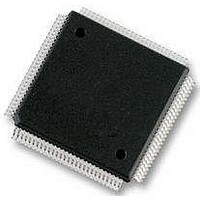
MC912D60CCPVE Freescale Semiconductor, MC912D60CCPVE Datasheet - Page 127

MC912D60CCPVE
Manufacturer Part Number
MC912D60CCPVE
Description
IC MCU 16BIT 112-LQFP
Manufacturer
Freescale Semiconductor
Series
HC12r
Datasheet
1.MC912D60ACFUE8.pdf
(460 pages)
Specifications of MC912D60CCPVE
Core Processor
CPU12
Core Size
16-Bit
Speed
8MHz
Connectivity
CAN, MI Bus, SCI, SPI
Peripherals
POR, PWM, WDT
Number Of I /o
68
Program Memory Size
60KB (60K x 8)
Program Memory Type
FLASH
Eeprom Size
1K x 8
Ram Size
2K x 8
Voltage - Supply (vcc/vdd)
4.5 V ~ 5.5 V
Data Converters
A/D 16x8/10b
Oscillator Type
Internal
Operating Temperature
-40°C ~ 85°C
Package / Case
112-LQFP
Processor Series
HC912D
Core
HC12
Data Bus Width
16 bit
Data Ram Size
2 KB
Interface Type
CAN, SCI, SPI
Maximum Clock Frequency
8 MHz
Number Of Programmable I/os
86
Maximum Operating Temperature
+ 85 C
Mounting Style
SMD/SMT
3rd Party Development Tools
EWHCS12
Minimum Operating Temperature
- 40 C
On-chip Adc
10 bit, 8 Channel
Lead Free Status / RoHS Status
Lead free / RoHS Compliant
Available stocks
Company
Part Number
Manufacturer
Quantity
Price
Company:
Part Number:
MC912D60CCPVE
Manufacturer:
FREESCAL
Quantity:
203
Company:
Part Number:
MC912D60CCPVE
Manufacturer:
Freescale Semiconductor
Quantity:
10 000
- Current page: 127 of 460
- Download datasheet (5Mb)
9.7.5 Central Processing Unit
9.7.6 Memory
9.7.7 Other Resources
9.8 Register Stacking
MC68HC912D60A — Rev. 3.1
Freescale Semiconductor
If the MCU comes out of reset in an expanded mode, port A and port B
are used for the address/data bus, and port E pins are normally used to
control the external bus (operation of port E pins can be affected by the
PEAR register). Out of reset, port G, port H, port P, port S, port T, port
CAN[7:2], port AD0 and port AD1 are all configured as general-purpose
inputs.
After reset, the CPU fetches a vector from the appropriate address, then
begins executing instructions. The stack pointer and other CPU registers
are indeterminate immediately after reset. The CCR X and I interrupt
mask bits are set to mask any interrupt requests. The S bit is also set to
inhibit the STOP instruction.
After reset, the internal register block is located from $0000 to $01FF,
RAM is at $0000 to $07FF, and EEPROM is located at $0C00 to $0FFF.
In single chip mode the two Flash EEPROM modules are located from
$1000 to $7FFF and $8000 to $FFFF.
The enhanced capture timer (ECT), pulse width modulation timer
(PWM), serial communications interfaces (SCI0 and SCI1), serial
peripheral interface (SPI), Scalable CAN (MSCAN) and analog-to-digital
converters (ATD0 and ATD1) are off after reset.
Once enabled, an interrupt request can be recognized at any time after
the I bit in the CCR is cleared. When an interrupt service request is
recognized, the CPU responds at the completion of the instruction being
executed. Interrupt latency varies according to the number of cycles
Resets and Interrupts
Resets and Interrupts
Register Stacking
Technical Data
127
Related parts for MC912D60CCPVE
Image
Part Number
Description
Manufacturer
Datasheet
Request
R
Part Number:
Description:
Manufacturer:
Freescale Semiconductor, Inc
Datasheet:
Part Number:
Description:
Manufacturer:
Freescale Semiconductor, Inc
Datasheet:
Part Number:
Description:
Manufacturer:
Freescale Semiconductor, Inc
Datasheet:
Part Number:
Description:
Manufacturer:
Freescale Semiconductor, Inc
Datasheet:
Part Number:
Description:
Manufacturer:
Freescale Semiconductor, Inc
Datasheet:
Part Number:
Description:
Manufacturer:
Freescale Semiconductor, Inc
Datasheet:
Part Number:
Description:
Manufacturer:
Freescale Semiconductor, Inc
Datasheet:
Part Number:
Description:
Manufacturer:
Freescale Semiconductor, Inc
Datasheet:
Part Number:
Description:
Manufacturer:
Freescale Semiconductor, Inc
Datasheet:
Part Number:
Description:
Manufacturer:
Freescale Semiconductor, Inc
Datasheet:
Part Number:
Description:
Manufacturer:
Freescale Semiconductor, Inc
Datasheet:
Part Number:
Description:
Manufacturer:
Freescale Semiconductor, Inc
Datasheet:
Part Number:
Description:
Manufacturer:
Freescale Semiconductor, Inc
Datasheet:
Part Number:
Description:
Manufacturer:
Freescale Semiconductor, Inc
Datasheet:
Part Number:
Description:
Manufacturer:
Freescale Semiconductor, Inc
Datasheet:


