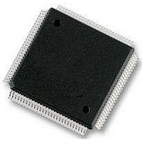
MC912D60CCPVE Freescale Semiconductor, MC912D60CCPVE Datasheet - Page 181

MC912D60CCPVE
Manufacturer Part Number
MC912D60CCPVE
Description
IC MCU 16BIT 112-LQFP
Manufacturer
Freescale Semiconductor
Series
HC12r
Datasheet
1.MC912D60ACFUE8.pdf
(460 pages)
Specifications of MC912D60CCPVE
Core Processor
CPU12
Core Size
16-Bit
Speed
8MHz
Connectivity
CAN, MI Bus, SCI, SPI
Peripherals
POR, PWM, WDT
Number Of I /o
68
Program Memory Size
60KB (60K x 8)
Program Memory Type
FLASH
Eeprom Size
1K x 8
Ram Size
2K x 8
Voltage - Supply (vcc/vdd)
4.5 V ~ 5.5 V
Data Converters
A/D 16x8/10b
Oscillator Type
Internal
Operating Temperature
-40°C ~ 85°C
Package / Case
112-LQFP
Processor Series
HC912D
Core
HC12
Data Bus Width
16 bit
Data Ram Size
2 KB
Interface Type
CAN, SCI, SPI
Maximum Clock Frequency
8 MHz
Number Of Programmable I/os
86
Maximum Operating Temperature
+ 85 C
Mounting Style
SMD/SMT
3rd Party Development Tools
EWHCS12
Minimum Operating Temperature
- 40 C
On-chip Adc
10 bit, 8 Channel
Lead Free Status / RoHS Status
Lead free / RoHS Compliant
Available stocks
Company
Part Number
Manufacturer
Quantity
Price
Company:
Part Number:
MC912D60CCPVE
Manufacturer:
FREESCAL
Quantity:
203
Company:
Part Number:
MC912D60CCPVE
Manufacturer:
Freescale Semiconductor
Quantity:
10 000
- Current page: 181 of 460
- Download datasheet (5Mb)
12.4.1.1 Clock Buffer Hysteresis
MC68HC912D60A — Rev. 3.1
Freescale Semiconductor
The input clock buffer uses an Operational Transconductance Amplifier
(labeled ‘OTA’ in the figure above) followed by a digital buffer to amplify
the input signal on the EXTAL pin into a full-swing clock for use by the
clock generation section of the microcontroller. There is an internal R-C
filter (composed of components RFLT2 and CFLT2 in the figure above),
which creates the DC value to which the EXTAL signal is compared. In
this manner, the clock input buffer can track changes in the EXTAL bias
voltage due to process variation as well as external factors such as
leakage.
Because the purpose of the clock input buffer is to amplify relatively low-
swing signals into a full-rail output, the gain of the OTA is very high. In
the configuration shown, this means that very small levels of noise can
be coupled onto the input of the clock buffer resulting in noise
amplification.
To remedy this issue, hysteresis was added to the OTA so that the circuit
could still provide the tolerance to leakage and the high gain required
without the noise sensitivity. Approximately 150mV of hysteresis was
added with a maximum hysteresis over process variation of 350mV. As
such, the clock input buffer will not respond to input signals until they
exceed the hysteresis level. At this point, the input signal due to
oscillation will dominate the total input waveform and narrow clock
pulses due to noise will be eliminated.
This circuit will limit the overall performance of the oscillator block only
in cases where the amplitude of oscillation is less than the level of
hysteresis. The minimum amplitude of oscillation is expected to be in
excess of 750mV and the maximum hysteresis is expected to be less
than 350mV, providing a factor of safety in excess of two.
•
•
The bias current to the amplifier was optimized for less variation
over process.
The input ESD resistor from EXTAL to the gate of the oscillator
amplifier was changed to provide a parallel path, reducing
parasitic phase shift in the oscillator.
Oscillator
MC68HC912D60C Colpitts Oscillator Specification
Technical Data
Oscillator
181
Related parts for MC912D60CCPVE
Image
Part Number
Description
Manufacturer
Datasheet
Request
R
Part Number:
Description:
Manufacturer:
Freescale Semiconductor, Inc
Datasheet:
Part Number:
Description:
Manufacturer:
Freescale Semiconductor, Inc
Datasheet:
Part Number:
Description:
Manufacturer:
Freescale Semiconductor, Inc
Datasheet:
Part Number:
Description:
Manufacturer:
Freescale Semiconductor, Inc
Datasheet:
Part Number:
Description:
Manufacturer:
Freescale Semiconductor, Inc
Datasheet:
Part Number:
Description:
Manufacturer:
Freescale Semiconductor, Inc
Datasheet:
Part Number:
Description:
Manufacturer:
Freescale Semiconductor, Inc
Datasheet:
Part Number:
Description:
Manufacturer:
Freescale Semiconductor, Inc
Datasheet:
Part Number:
Description:
Manufacturer:
Freescale Semiconductor, Inc
Datasheet:
Part Number:
Description:
Manufacturer:
Freescale Semiconductor, Inc
Datasheet:
Part Number:
Description:
Manufacturer:
Freescale Semiconductor, Inc
Datasheet:
Part Number:
Description:
Manufacturer:
Freescale Semiconductor, Inc
Datasheet:
Part Number:
Description:
Manufacturer:
Freescale Semiconductor, Inc
Datasheet:
Part Number:
Description:
Manufacturer:
Freescale Semiconductor, Inc
Datasheet:
Part Number:
Description:
Manufacturer:
Freescale Semiconductor, Inc
Datasheet:


