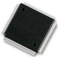
MC912D60CCPVE Freescale Semiconductor, MC912D60CCPVE Datasheet - Page 198

MC912D60CCPVE
Manufacturer Part Number
MC912D60CCPVE
Description
IC MCU 16BIT 112-LQFP
Manufacturer
Freescale Semiconductor
Series
HC12r
Datasheet
1.MC912D60ACFUE8.pdf
(460 pages)
Specifications of MC912D60CCPVE
Core Processor
CPU12
Core Size
16-Bit
Speed
8MHz
Connectivity
CAN, MI Bus, SCI, SPI
Peripherals
POR, PWM, WDT
Number Of I /o
68
Program Memory Size
60KB (60K x 8)
Program Memory Type
FLASH
Eeprom Size
1K x 8
Ram Size
2K x 8
Voltage - Supply (vcc/vdd)
4.5 V ~ 5.5 V
Data Converters
A/D 16x8/10b
Oscillator Type
Internal
Operating Temperature
-40°C ~ 85°C
Package / Case
112-LQFP
Processor Series
HC912D
Core
HC12
Data Bus Width
16 bit
Data Ram Size
2 KB
Interface Type
CAN, SCI, SPI
Maximum Clock Frequency
8 MHz
Number Of Programmable I/os
86
Maximum Operating Temperature
+ 85 C
Mounting Style
SMD/SMT
3rd Party Development Tools
EWHCS12
Minimum Operating Temperature
- 40 C
On-chip Adc
10 bit, 8 Channel
Lead Free Status / RoHS Status
Lead free / RoHS Compliant
Available stocks
Company
Part Number
Manufacturer
Quantity
Price
Company:
Part Number:
MC912D60CCPVE
Manufacturer:
FREESCAL
Quantity:
203
Company:
Part Number:
MC912D60CCPVE
Manufacturer:
Freescale Semiconductor
Quantity:
10 000
- Current page: 198 of 460
- Download datasheet (5Mb)
Oscillator
12.5.1.3 Bias Current Process Optimization
12.5.1.4 Input ESD Resistor Path Modification
Technical Data
198
For proper oscillation, the gain margin of the oscillator must exceed one
or the circuit will not oscillate. Process variance in the bias current (which
controls the gain of the amplifier) can cause the gain margin to be much
lower than typical. This can be as a result of either too much or too little
current.
To reduce the process sensitivity of the gain, the material of the device
that sets the bias current was changed to a material with tighter process
and temperature control. As a result, the transconductance and Ibias
variances are more limited than in the previous design.
To satisfy the condition of oscillation, the oscillator circuit must not only
provide the correct amount of gain but also the correct amount of phase
shift. In the Pierce configuration, the phase shift due to parasitics in the
input path to the gate of the transconductance amplifier must be as low
as possible. In the original configuration, the parasitic capacitance of the
clock input buffer (OTA), automatic Loop Control circuit (ALC), and input
resistor (RFLT) reacted with the input resistance to cause a large phase
shift.
To reduce the phase shift, the input ESD resistor (marked RESD in the
figure above) was changed from a single path to the input circuitry (the
ALC and the OTA) and oscillator transconductance amplifier (marked
GM in the figure above) to a parallel path. In this configuration, the only
capacitance causing a phase shift on the input to the transconductance
device is due to the transconductance device itself.
Oscillator
MC68HC912D60A — Rev. 3.1
Freescale Semiconductor
Related parts for MC912D60CCPVE
Image
Part Number
Description
Manufacturer
Datasheet
Request
R
Part Number:
Description:
Manufacturer:
Freescale Semiconductor, Inc
Datasheet:
Part Number:
Description:
Manufacturer:
Freescale Semiconductor, Inc
Datasheet:
Part Number:
Description:
Manufacturer:
Freescale Semiconductor, Inc
Datasheet:
Part Number:
Description:
Manufacturer:
Freescale Semiconductor, Inc
Datasheet:
Part Number:
Description:
Manufacturer:
Freescale Semiconductor, Inc
Datasheet:
Part Number:
Description:
Manufacturer:
Freescale Semiconductor, Inc
Datasheet:
Part Number:
Description:
Manufacturer:
Freescale Semiconductor, Inc
Datasheet:
Part Number:
Description:
Manufacturer:
Freescale Semiconductor, Inc
Datasheet:
Part Number:
Description:
Manufacturer:
Freescale Semiconductor, Inc
Datasheet:
Part Number:
Description:
Manufacturer:
Freescale Semiconductor, Inc
Datasheet:
Part Number:
Description:
Manufacturer:
Freescale Semiconductor, Inc
Datasheet:
Part Number:
Description:
Manufacturer:
Freescale Semiconductor, Inc
Datasheet:
Part Number:
Description:
Manufacturer:
Freescale Semiconductor, Inc
Datasheet:
Part Number:
Description:
Manufacturer:
Freescale Semiconductor, Inc
Datasheet:
Part Number:
Description:
Manufacturer:
Freescale Semiconductor, Inc
Datasheet:


