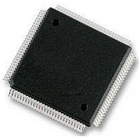
MC912D60CCPVE Freescale Semiconductor, MC912D60CCPVE Datasheet - Page 221

MC912D60CCPVE
Manufacturer Part Number
MC912D60CCPVE
Description
IC MCU 16BIT 112-LQFP
Manufacturer
Freescale Semiconductor
Series
HC12r
Datasheet
1.MC912D60ACFUE8.pdf
(460 pages)
Specifications of MC912D60CCPVE
Core Processor
CPU12
Core Size
16-Bit
Speed
8MHz
Connectivity
CAN, MI Bus, SCI, SPI
Peripherals
POR, PWM, WDT
Number Of I /o
68
Program Memory Size
60KB (60K x 8)
Program Memory Type
FLASH
Eeprom Size
1K x 8
Ram Size
2K x 8
Voltage - Supply (vcc/vdd)
4.5 V ~ 5.5 V
Data Converters
A/D 16x8/10b
Oscillator Type
Internal
Operating Temperature
-40°C ~ 85°C
Package / Case
112-LQFP
Processor Series
HC912D
Core
HC12
Data Bus Width
16 bit
Data Ram Size
2 KB
Interface Type
CAN, SCI, SPI
Maximum Clock Frequency
8 MHz
Number Of Programmable I/os
86
Maximum Operating Temperature
+ 85 C
Mounting Style
SMD/SMT
3rd Party Development Tools
EWHCS12
Minimum Operating Temperature
- 40 C
On-chip Adc
10 bit, 8 Channel
Lead Free Status / RoHS Status
Lead free / RoHS Compliant
Available stocks
Company
Part Number
Manufacturer
Quantity
Price
Company:
Part Number:
MC912D60CCPVE
Manufacturer:
FREESCAL
Quantity:
203
Company:
Part Number:
MC912D60CCPVE
Manufacturer:
Freescale Semiconductor
Quantity:
10 000
- Current page: 221 of 460
- Download datasheet (5Mb)
PORTP — Port P Data Register
DDRP — Port P Data Direction Register
MC68HC912D60A — Rev. 3.1
Freescale Semiconductor
RESET:
RESET:
PWM
DDP7
Bit 7
Bit 7
PP7
0
–
–
DDP6
PP6
6
–
–
6
0
PORTP can be read anytime.
PWM functions share port P pins 3 to 0 and take precedence over the
general-purpose port when enabled.
When configured as input, a read will return the pin level.
When configured as output, a read will return the latched output data.
A write will drive associated pins only if configured for output and the
corresponding PWM channel is not enabled.
After reset, all pins are general-purpose, high-impedance inputs.
DDRP determines pin direction of port P when used for general-purpose
I/O.
Read and write anytime.
DDRP[7:0] — Data Direction Port P pin 7-0
0 = I/O pin configured as high impedance input
1 = I/O pin configured for output.
DDP5
PP5
5
0
5
–
–
Pulse Width Modulator
DDP4
PP4
4
–
–
4
0
PWM3
DDP3
PP3
3
0
3
–
PWM2
DDP2
PP2
2
–
2
0
PWM1
DDP1
PP1
1
1
–
0
PWM Register Description
Pulse Width Modulator
PWM0
DDP0
Bit 0
Bit 0
PP0
–
0
Technical Data
$0056
$0057
221
Related parts for MC912D60CCPVE
Image
Part Number
Description
Manufacturer
Datasheet
Request
R
Part Number:
Description:
Manufacturer:
Freescale Semiconductor, Inc
Datasheet:
Part Number:
Description:
Manufacturer:
Freescale Semiconductor, Inc
Datasheet:
Part Number:
Description:
Manufacturer:
Freescale Semiconductor, Inc
Datasheet:
Part Number:
Description:
Manufacturer:
Freescale Semiconductor, Inc
Datasheet:
Part Number:
Description:
Manufacturer:
Freescale Semiconductor, Inc
Datasheet:
Part Number:
Description:
Manufacturer:
Freescale Semiconductor, Inc
Datasheet:
Part Number:
Description:
Manufacturer:
Freescale Semiconductor, Inc
Datasheet:
Part Number:
Description:
Manufacturer:
Freescale Semiconductor, Inc
Datasheet:
Part Number:
Description:
Manufacturer:
Freescale Semiconductor, Inc
Datasheet:
Part Number:
Description:
Manufacturer:
Freescale Semiconductor, Inc
Datasheet:
Part Number:
Description:
Manufacturer:
Freescale Semiconductor, Inc
Datasheet:
Part Number:
Description:
Manufacturer:
Freescale Semiconductor, Inc
Datasheet:
Part Number:
Description:
Manufacturer:
Freescale Semiconductor, Inc
Datasheet:
Part Number:
Description:
Manufacturer:
Freescale Semiconductor, Inc
Datasheet:
Part Number:
Description:
Manufacturer:
Freescale Semiconductor, Inc
Datasheet:


