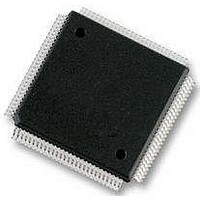
MC912D60CCPVE Freescale Semiconductor, MC912D60CCPVE Datasheet - Page 255

MC912D60CCPVE
Manufacturer Part Number
MC912D60CCPVE
Description
IC MCU 16BIT 112-LQFP
Manufacturer
Freescale Semiconductor
Series
HC12r
Datasheet
1.MC912D60ACFUE8.pdf
(460 pages)
Specifications of MC912D60CCPVE
Core Processor
CPU12
Core Size
16-Bit
Speed
8MHz
Connectivity
CAN, MI Bus, SCI, SPI
Peripherals
POR, PWM, WDT
Number Of I /o
68
Program Memory Size
60KB (60K x 8)
Program Memory Type
FLASH
Eeprom Size
1K x 8
Ram Size
2K x 8
Voltage - Supply (vcc/vdd)
4.5 V ~ 5.5 V
Data Converters
A/D 16x8/10b
Oscillator Type
Internal
Operating Temperature
-40°C ~ 85°C
Package / Case
112-LQFP
Processor Series
HC912D
Core
HC12
Data Bus Width
16 bit
Data Ram Size
2 KB
Interface Type
CAN, SCI, SPI
Maximum Clock Frequency
8 MHz
Number Of Programmable I/os
86
Maximum Operating Temperature
+ 85 C
Mounting Style
SMD/SMT
3rd Party Development Tools
EWHCS12
Minimum Operating Temperature
- 40 C
On-chip Adc
10 bit, 8 Channel
Lead Free Status / RoHS Status
Lead free / RoHS Compliant
Available stocks
Company
Part Number
Manufacturer
Quantity
Price
Company:
Part Number:
MC912D60CCPVE
Manufacturer:
FREESCAL
Quantity:
203
Company:
Part Number:
MC912D60CCPVE
Manufacturer:
Freescale Semiconductor
Quantity:
10 000
- Current page: 255 of 460
- Download datasheet (5Mb)
PORTT — Timer Port Data Register
MC68HC912D60A — Rev. 3.1
Freescale Semiconductor
RESET:
TIMER
PORT
I/OC7
BIT 7
PT7
NOTE:
0
I/OC6
PT6
6
0
Since the Output Compare 7 shares the pin with Pulse Accumulator
input, the only way for Pulse accumulator to receive an independent
input from Output Compare 7 is setting both OM7 & OL7 to be zero, and
also OC7M7 in OC7M register to be zero.
OC7 is still able to reset the counter if enabled while PT7 is used as input
to Pulse Accumulator.
PORTT can be read anytime. When configured as an input, a read will
return the pin level. When configured as an output, a read will return the
latched output data.
Writes do not change pin state when the pin is configured for timer
output. The minimum pulse width for pulse accumulator input should
always be greater than the width of two module clocks due to input
synchronizer circuitry. The minimum pulse width for the input capture
should always be greater than the width of two module clocks due to
input synchronizer circuitry.
Read: any time (inputs return pin level; outputs return data register
contents)
Write: data stored in an internal latch (drives pins only if configured for
output)
I/OC5
PT5
5
0
Enhanced Capture Timer
I/OC4
PT4
4
0
I/OC3
PT3
3
0
I/OC2
PT2
2
0
I/OC1
PT1
1
0
Enhanced Capture Timer
I/OC0
BIT 0
PT0
0
Timer Registers
Technical Data
$00AE
255
Related parts for MC912D60CCPVE
Image
Part Number
Description
Manufacturer
Datasheet
Request
R
Part Number:
Description:
Manufacturer:
Freescale Semiconductor, Inc
Datasheet:
Part Number:
Description:
Manufacturer:
Freescale Semiconductor, Inc
Datasheet:
Part Number:
Description:
Manufacturer:
Freescale Semiconductor, Inc
Datasheet:
Part Number:
Description:
Manufacturer:
Freescale Semiconductor, Inc
Datasheet:
Part Number:
Description:
Manufacturer:
Freescale Semiconductor, Inc
Datasheet:
Part Number:
Description:
Manufacturer:
Freescale Semiconductor, Inc
Datasheet:
Part Number:
Description:
Manufacturer:
Freescale Semiconductor, Inc
Datasheet:
Part Number:
Description:
Manufacturer:
Freescale Semiconductor, Inc
Datasheet:
Part Number:
Description:
Manufacturer:
Freescale Semiconductor, Inc
Datasheet:
Part Number:
Description:
Manufacturer:
Freescale Semiconductor, Inc
Datasheet:
Part Number:
Description:
Manufacturer:
Freescale Semiconductor, Inc
Datasheet:
Part Number:
Description:
Manufacturer:
Freescale Semiconductor, Inc
Datasheet:
Part Number:
Description:
Manufacturer:
Freescale Semiconductor, Inc
Datasheet:
Part Number:
Description:
Manufacturer:
Freescale Semiconductor, Inc
Datasheet:
Part Number:
Description:
Manufacturer:
Freescale Semiconductor, Inc
Datasheet:


