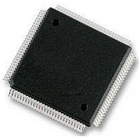
MC912D60CCPVE Freescale Semiconductor, MC912D60CCPVE Datasheet - Page 276

MC912D60CCPVE
Manufacturer Part Number
MC912D60CCPVE
Description
IC MCU 16BIT 112-LQFP
Manufacturer
Freescale Semiconductor
Series
HC12r
Datasheet
1.MC912D60ACFUE8.pdf
(460 pages)
Specifications of MC912D60CCPVE
Core Processor
CPU12
Core Size
16-Bit
Speed
8MHz
Connectivity
CAN, MI Bus, SCI, SPI
Peripherals
POR, PWM, WDT
Number Of I /o
68
Program Memory Size
60KB (60K x 8)
Program Memory Type
FLASH
Eeprom Size
1K x 8
Ram Size
2K x 8
Voltage - Supply (vcc/vdd)
4.5 V ~ 5.5 V
Data Converters
A/D 16x8/10b
Oscillator Type
Internal
Operating Temperature
-40°C ~ 85°C
Package / Case
112-LQFP
Processor Series
HC912D
Core
HC12
Data Bus Width
16 bit
Data Ram Size
2 KB
Interface Type
CAN, SCI, SPI
Maximum Clock Frequency
8 MHz
Number Of Programmable I/os
86
Maximum Operating Temperature
+ 85 C
Mounting Style
SMD/SMT
3rd Party Development Tools
EWHCS12
Minimum Operating Temperature
- 40 C
On-chip Adc
10 bit, 8 Channel
Lead Free Status / RoHS Status
Lead free / RoHS Compliant
Available stocks
Company
Part Number
Manufacturer
Quantity
Price
Company:
Part Number:
MC912D60CCPVE
Manufacturer:
FREESCAL
Quantity:
203
Company:
Part Number:
MC912D60CCPVE
Manufacturer:
Freescale Semiconductor
Quantity:
10 000
- Current page: 276 of 460
- Download datasheet (5Mb)
Multiple Serial Interface
15.5 Serial Peripheral Interface (SPI)
15.5.1 SPI Baud Rate Generation
15.5.2 SPI Operation
Technical Data
276
The serial peripheral interface allows the MC68HC912D60A to
communicate synchronously with peripheral devices and other
microprocessors. The SPI system in the MC68HC912D60A can operate
as a master or as a slave. The SPI is also capable of interprocessor
communications in a multiple master system.
When the SPI is enabled, all pins that are defined by the configuration
as inputs will be inputs regardless of the state of the DDRS bits for those
pins. All pins that are defined as SPI outputs will be outputs only if the
DDRS bits for those pins are set. Any SPI output whose corresponding
DDRS bit is cleared can be used as a general-purpose input.
A bidirectional serial pin is possible using the DDRS as the direction
control.
The E Clock is input to a divider series and the resulting SPI clock rate
may be selected to be E divided by 2, 4, 8, 16, 32, 64, 128 or 256. Three
bits in the SP0BR register control the SPI clock rate. This baud rate
generator is activated only when SPI is in the master mode and serial
transfer is taking place. Otherwise this divider is disabled to save power.
In the SPI system the 8-bit data register in the master and the 8-bit data
register in the slave are linked to form a distributed 16-bit register. When
a data transfer operation is performed, this 16-bit register is serially
shifted eight bit positions by the SCK clock from the master so the data
is effectively exchanged between the master and the slave. Data written
to the SP0DR register of the master becomes the output data for the
slave and data read from the SP0DR register of the master after a
transfer operation is the input data from the slave.
Multiple Serial Interface
MC68HC912D60A — Rev. 3.1
Freescale Semiconductor
Related parts for MC912D60CCPVE
Image
Part Number
Description
Manufacturer
Datasheet
Request
R
Part Number:
Description:
Manufacturer:
Freescale Semiconductor, Inc
Datasheet:
Part Number:
Description:
Manufacturer:
Freescale Semiconductor, Inc
Datasheet:
Part Number:
Description:
Manufacturer:
Freescale Semiconductor, Inc
Datasheet:
Part Number:
Description:
Manufacturer:
Freescale Semiconductor, Inc
Datasheet:
Part Number:
Description:
Manufacturer:
Freescale Semiconductor, Inc
Datasheet:
Part Number:
Description:
Manufacturer:
Freescale Semiconductor, Inc
Datasheet:
Part Number:
Description:
Manufacturer:
Freescale Semiconductor, Inc
Datasheet:
Part Number:
Description:
Manufacturer:
Freescale Semiconductor, Inc
Datasheet:
Part Number:
Description:
Manufacturer:
Freescale Semiconductor, Inc
Datasheet:
Part Number:
Description:
Manufacturer:
Freescale Semiconductor, Inc
Datasheet:
Part Number:
Description:
Manufacturer:
Freescale Semiconductor, Inc
Datasheet:
Part Number:
Description:
Manufacturer:
Freescale Semiconductor, Inc
Datasheet:
Part Number:
Description:
Manufacturer:
Freescale Semiconductor, Inc
Datasheet:
Part Number:
Description:
Manufacturer:
Freescale Semiconductor, Inc
Datasheet:
Part Number:
Description:
Manufacturer:
Freescale Semiconductor, Inc
Datasheet:


