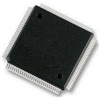
MC912D60CCPVE Freescale Semiconductor, MC912D60CCPVE Datasheet - Page 282

MC912D60CCPVE
Manufacturer Part Number
MC912D60CCPVE
Description
IC MCU 16BIT 112-LQFP
Manufacturer
Freescale Semiconductor
Series
HC12r
Datasheet
1.MC912D60ACFUE8.pdf
(460 pages)
Specifications of MC912D60CCPVE
Core Processor
CPU12
Core Size
16-Bit
Speed
8MHz
Connectivity
CAN, MI Bus, SCI, SPI
Peripherals
POR, PWM, WDT
Number Of I /o
68
Program Memory Size
60KB (60K x 8)
Program Memory Type
FLASH
Eeprom Size
1K x 8
Ram Size
2K x 8
Voltage - Supply (vcc/vdd)
4.5 V ~ 5.5 V
Data Converters
A/D 16x8/10b
Oscillator Type
Internal
Operating Temperature
-40°C ~ 85°C
Package / Case
112-LQFP
Processor Series
HC912D
Core
HC12
Data Bus Width
16 bit
Data Ram Size
2 KB
Interface Type
CAN, SCI, SPI
Maximum Clock Frequency
8 MHz
Number Of Programmable I/os
86
Maximum Operating Temperature
+ 85 C
Mounting Style
SMD/SMT
3rd Party Development Tools
EWHCS12
Minimum Operating Temperature
- 40 C
On-chip Adc
10 bit, 8 Channel
Lead Free Status / RoHS Status
Lead free / RoHS Compliant
Available stocks
Company
Part Number
Manufacturer
Quantity
Price
Company:
Part Number:
MC912D60CCPVE
Manufacturer:
FREESCAL
Quantity:
203
Company:
Part Number:
MC912D60CCPVE
Manufacturer:
Freescale Semiconductor
Quantity:
10 000
- Current page: 282 of 460
- Download datasheet (5Mb)
Multiple Serial Interface
SP0CR2 — SPI Control Register 2
Technical Data
282
RESET:
Bit 7
0
0
1. The serial pin control 0 bit enables bidirectional configurations.
2. Slave output is enabled if DDS4 = 1, SS = 0 and MSTR = 0. (#1, #3)
3. Master output is enabled if DDS5 = 1 and MSTR = 1. (#2, #4)
4. SCK output is enabled if DDS6 = 1 and MSTR = 1. (#2, #4)
5. SS output is enabled if DDS7 = 1, SSOE = 1 and MSTR = 1. (#2, #4)
#1
#2
#3
#4
Pin Mode
Bidirectional
6
0
0
Read or write anytime.
SPSWAI — Serial Interface Stop in WAIT mode
SPC0 — Serial Pin Control 0
Normal
Normally data is transferred most significant bit first.This bit does not
affect the position of the MSB and LSB in the data register. Reads and
writes of the data register will always have MSB in bit 7.
This bit decides serial pin configurations with MSTR control bit.
0 = Serial interface clock operates normally
1 = Halt serial interface clock generation in WAIT mode
5
0
0
SPC0
Multiple Serial Interface
0
1
(1)
4
0
0
MSTR
0
1
0
1
3
0
0
Slave Out
Master In Master Out
Slave I/O
MISO
GPI/O
(2)
2
0
0
Master I/O
MOSI
Slave In
GPI/O
SPSWAI
MC68HC912D60A — Rev. 3.1
(3)
1
0
Freescale Semiconductor
SCK Out
SCK Out
SCK In
SCK In
SCK
SPC0
Bit 0
0
(4)
SS I/O
SS I/O
SS In
SS In
SS
$00D1
(5)
Related parts for MC912D60CCPVE
Image
Part Number
Description
Manufacturer
Datasheet
Request
R
Part Number:
Description:
Manufacturer:
Freescale Semiconductor, Inc
Datasheet:
Part Number:
Description:
Manufacturer:
Freescale Semiconductor, Inc
Datasheet:
Part Number:
Description:
Manufacturer:
Freescale Semiconductor, Inc
Datasheet:
Part Number:
Description:
Manufacturer:
Freescale Semiconductor, Inc
Datasheet:
Part Number:
Description:
Manufacturer:
Freescale Semiconductor, Inc
Datasheet:
Part Number:
Description:
Manufacturer:
Freescale Semiconductor, Inc
Datasheet:
Part Number:
Description:
Manufacturer:
Freescale Semiconductor, Inc
Datasheet:
Part Number:
Description:
Manufacturer:
Freescale Semiconductor, Inc
Datasheet:
Part Number:
Description:
Manufacturer:
Freescale Semiconductor, Inc
Datasheet:
Part Number:
Description:
Manufacturer:
Freescale Semiconductor, Inc
Datasheet:
Part Number:
Description:
Manufacturer:
Freescale Semiconductor, Inc
Datasheet:
Part Number:
Description:
Manufacturer:
Freescale Semiconductor, Inc
Datasheet:
Part Number:
Description:
Manufacturer:
Freescale Semiconductor, Inc
Datasheet:
Part Number:
Description:
Manufacturer:
Freescale Semiconductor, Inc
Datasheet:
Part Number:
Description:
Manufacturer:
Freescale Semiconductor, Inc
Datasheet:


