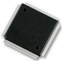
MC912D60CCPVE Freescale Semiconductor, MC912D60CCPVE Datasheet - Page 291

MC912D60CCPVE
Manufacturer Part Number
MC912D60CCPVE
Description
IC MCU 16BIT 112-LQFP
Manufacturer
Freescale Semiconductor
Series
HC12r
Datasheet
1.MC912D60ACFUE8.pdf
(460 pages)
Specifications of MC912D60CCPVE
Core Processor
CPU12
Core Size
16-Bit
Speed
8MHz
Connectivity
CAN, MI Bus, SCI, SPI
Peripherals
POR, PWM, WDT
Number Of I /o
68
Program Memory Size
60KB (60K x 8)
Program Memory Type
FLASH
Eeprom Size
1K x 8
Ram Size
2K x 8
Voltage - Supply (vcc/vdd)
4.5 V ~ 5.5 V
Data Converters
A/D 16x8/10b
Oscillator Type
Internal
Operating Temperature
-40°C ~ 85°C
Package / Case
112-LQFP
Processor Series
HC912D
Core
HC12
Data Bus Width
16 bit
Data Ram Size
2 KB
Interface Type
CAN, SCI, SPI
Maximum Clock Frequency
8 MHz
Number Of Programmable I/os
86
Maximum Operating Temperature
+ 85 C
Mounting Style
SMD/SMT
3rd Party Development Tools
EWHCS12
Minimum Operating Temperature
- 40 C
On-chip Adc
10 bit, 8 Channel
Lead Free Status / RoHS Status
Lead free / RoHS Compliant
Available stocks
Company
Part Number
Manufacturer
Quantity
Price
Company:
Part Number:
MC912D60CCPVE
Manufacturer:
FREESCAL
Quantity:
203
Company:
Part Number:
MC912D60CCPVE
Manufacturer:
Freescale Semiconductor
Quantity:
10 000
- Current page: 291 of 460
- Download datasheet (5Mb)
16.3.1 The push field
16.3.2 The pull field
16.4 Biphase coding
MC68HC912D60A — Rev. 3.1
Freescale Semiconductor
The push field consists of a start bit, a push synchronization bit, a push
data field and a push address field. The start consists of three time slots
having the dominant logical state ‘0’. The start marks the beginning of
the message frame by violation of the rule of the Manchester code. The
push synchronization bit consists of a biphase coded ‘0’. Biphase coding
will be discussed later. The push data field consists of five bits of biphase
coded data. The push address consists of three bits of biphase coded
data. Data and address are written to the lower byte of the SCI data
register (SC0DRL). The push data occupies the lower five bits and the
push address occupies the upper three bits of the register.
The pull field consists of a pull synchronization bit, a pull data field and
an end of frame. The pull synchronization bit is a biphase coded ‘1’ and
is initiated by the MCU during the time slot after the last address bit of
the push field. The pull data field consists of an NRZ coded transmission,
each bit taking one time slot. Once shifted in, the pull data is stored in
the lower byte of the SCI data register (SC0DRL). The end-of-frame field
is a square wave signal having a typical frequency of 20kHz ± 1%
tolerance (i.e. the bit rate of the push field) when the data sent to the
selected device is valid.
Manchester biphase L coding is used for the push field bits. Each bit
requires two time slots to encode the logic value of the bit. This encoding
allows the detection of a single error at the time slot level. Bits are
encoded as follows:
0 = In the first time slot, the logic level is set to one, followed by a
1 = In the first time slot, the logic level is set to zero, followed by a
logic level zero in the second time slot.
logic level one in the second time slot.
Freescale Interconnect Bus
Freescale Interconnect Bus
Biphase coding
Technical Data
291
Related parts for MC912D60CCPVE
Image
Part Number
Description
Manufacturer
Datasheet
Request
R
Part Number:
Description:
Manufacturer:
Freescale Semiconductor, Inc
Datasheet:
Part Number:
Description:
Manufacturer:
Freescale Semiconductor, Inc
Datasheet:
Part Number:
Description:
Manufacturer:
Freescale Semiconductor, Inc
Datasheet:
Part Number:
Description:
Manufacturer:
Freescale Semiconductor, Inc
Datasheet:
Part Number:
Description:
Manufacturer:
Freescale Semiconductor, Inc
Datasheet:
Part Number:
Description:
Manufacturer:
Freescale Semiconductor, Inc
Datasheet:
Part Number:
Description:
Manufacturer:
Freescale Semiconductor, Inc
Datasheet:
Part Number:
Description:
Manufacturer:
Freescale Semiconductor, Inc
Datasheet:
Part Number:
Description:
Manufacturer:
Freescale Semiconductor, Inc
Datasheet:
Part Number:
Description:
Manufacturer:
Freescale Semiconductor, Inc
Datasheet:
Part Number:
Description:
Manufacturer:
Freescale Semiconductor, Inc
Datasheet:
Part Number:
Description:
Manufacturer:
Freescale Semiconductor, Inc
Datasheet:
Part Number:
Description:
Manufacturer:
Freescale Semiconductor, Inc
Datasheet:
Part Number:
Description:
Manufacturer:
Freescale Semiconductor, Inc
Datasheet:
Part Number:
Description:
Manufacturer:
Freescale Semiconductor, Inc
Datasheet:


