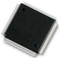
MC912D60CCPVE Freescale Semiconductor, MC912D60CCPVE Datasheet - Page 321

MC912D60CCPVE
Manufacturer Part Number
MC912D60CCPVE
Description
IC MCU 16BIT 112-LQFP
Manufacturer
Freescale Semiconductor
Series
HC12r
Datasheet
1.MC912D60ACFUE8.pdf
(460 pages)
Specifications of MC912D60CCPVE
Core Processor
CPU12
Core Size
16-Bit
Speed
8MHz
Connectivity
CAN, MI Bus, SCI, SPI
Peripherals
POR, PWM, WDT
Number Of I /o
68
Program Memory Size
60KB (60K x 8)
Program Memory Type
FLASH
Eeprom Size
1K x 8
Ram Size
2K x 8
Voltage - Supply (vcc/vdd)
4.5 V ~ 5.5 V
Data Converters
A/D 16x8/10b
Oscillator Type
Internal
Operating Temperature
-40°C ~ 85°C
Package / Case
112-LQFP
Processor Series
HC912D
Core
HC12
Data Bus Width
16 bit
Data Ram Size
2 KB
Interface Type
CAN, SCI, SPI
Maximum Clock Frequency
8 MHz
Number Of Programmable I/os
86
Maximum Operating Temperature
+ 85 C
Mounting Style
SMD/SMT
3rd Party Development Tools
EWHCS12
Minimum Operating Temperature
- 40 C
On-chip Adc
10 bit, 8 Channel
Lead Free Status / RoHS Status
Lead free / RoHS Compliant
Available stocks
Company
Part Number
Manufacturer
Quantity
Price
Company:
Part Number:
MC912D60CCPVE
Manufacturer:
FREESCAL
Quantity:
203
Company:
Part Number:
MC912D60CCPVE
Manufacturer:
Freescale Semiconductor
Quantity:
10 000
- Current page: 321 of 460
- Download datasheet (5Mb)
17.10 Clock System
MC68HC912D60A — Rev. 3.1
Freescale Semiconductor
receives the frames being sent by itself, a timer signal is also generated
after a successful transmission.
The previously described timer signal can be routed into the on-chip
timer interface module (ECT). This signal is connected to the Timer n
Channel m input
bit in the CMCR0.
After timer n has been programmed to capture rising edge events, it can
be used under software control to generate 16-bit time stamps which can
be stored with the received message.
Figure 17-7
circuitry. With this flexible clocking scheme the msCAN12 is able to
handle CAN bus rates ranging from 10 kbps up to 1 Mbps.
The clock source bit (CLKSRC) in the msCAN12 module control register
(CMCR1) (see
whether the msCAN12 is connected to the output of the crystal oscillator
(EXTALi) or to a clock twice as fast as the system clock (ECLK).
The clock source has to be chosen such that the tight oscillator tolerance
requirements (up to 0.4%) of the CAN protocol are met. Additionally, for
high CAN bus rates (1 Mbps), a 50% duty cycle of the clock is required.
1. The timer channel being used for the timer link is integration dependent.
SYSCLK
EXTALi
shows the structure of the msCAN12 clock generation
msCAN12 Bus Timing Register 0
MSCAN Controller
(1)
under the control of the timer link enable (TLNKEN)
Figure 17-7. Clocking Scheme
CLKSRC
CGM
CGMCANCLK
msCAN12
Prescaler
(1...64)
CLKSRC
(CBTR0)) defines
Time quanta
MSCAN Controller
clock
Technical Data
Clock System
321
Related parts for MC912D60CCPVE
Image
Part Number
Description
Manufacturer
Datasheet
Request
R
Part Number:
Description:
Manufacturer:
Freescale Semiconductor, Inc
Datasheet:
Part Number:
Description:
Manufacturer:
Freescale Semiconductor, Inc
Datasheet:
Part Number:
Description:
Manufacturer:
Freescale Semiconductor, Inc
Datasheet:
Part Number:
Description:
Manufacturer:
Freescale Semiconductor, Inc
Datasheet:
Part Number:
Description:
Manufacturer:
Freescale Semiconductor, Inc
Datasheet:
Part Number:
Description:
Manufacturer:
Freescale Semiconductor, Inc
Datasheet:
Part Number:
Description:
Manufacturer:
Freescale Semiconductor, Inc
Datasheet:
Part Number:
Description:
Manufacturer:
Freescale Semiconductor, Inc
Datasheet:
Part Number:
Description:
Manufacturer:
Freescale Semiconductor, Inc
Datasheet:
Part Number:
Description:
Manufacturer:
Freescale Semiconductor, Inc
Datasheet:
Part Number:
Description:
Manufacturer:
Freescale Semiconductor, Inc
Datasheet:
Part Number:
Description:
Manufacturer:
Freescale Semiconductor, Inc
Datasheet:
Part Number:
Description:
Manufacturer:
Freescale Semiconductor, Inc
Datasheet:
Part Number:
Description:
Manufacturer:
Freescale Semiconductor, Inc
Datasheet:
Part Number:
Description:
Manufacturer:
Freescale Semiconductor, Inc
Datasheet:


