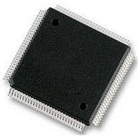
MC912D60CCPVE Freescale Semiconductor, MC912D60CCPVE Datasheet - Page 349

MC912D60CCPVE
Manufacturer Part Number
MC912D60CCPVE
Description
IC MCU 16BIT 112-LQFP
Manufacturer
Freescale Semiconductor
Series
HC12r
Datasheet
1.MC912D60ACFUE8.pdf
(460 pages)
Specifications of MC912D60CCPVE
Core Processor
CPU12
Core Size
16-Bit
Speed
8MHz
Connectivity
CAN, MI Bus, SCI, SPI
Peripherals
POR, PWM, WDT
Number Of I /o
68
Program Memory Size
60KB (60K x 8)
Program Memory Type
FLASH
Eeprom Size
1K x 8
Ram Size
2K x 8
Voltage - Supply (vcc/vdd)
4.5 V ~ 5.5 V
Data Converters
A/D 16x8/10b
Oscillator Type
Internal
Operating Temperature
-40°C ~ 85°C
Package / Case
112-LQFP
Processor Series
HC912D
Core
HC12
Data Bus Width
16 bit
Data Ram Size
2 KB
Interface Type
CAN, SCI, SPI
Maximum Clock Frequency
8 MHz
Number Of Programmable I/os
86
Maximum Operating Temperature
+ 85 C
Mounting Style
SMD/SMT
3rd Party Development Tools
EWHCS12
Minimum Operating Temperature
- 40 C
On-chip Adc
10 bit, 8 Channel
Lead Free Status / RoHS Status
Lead free / RoHS Compliant
Available stocks
Company
Part Number
Manufacturer
Quantity
Price
Company:
Part Number:
MC912D60CCPVE
Manufacturer:
FREESCAL
Quantity:
203
Company:
Part Number:
MC912D60CCPVE
Manufacturer:
Freescale Semiconductor
Quantity:
10 000
- Current page: 349 of 460
- Download datasheet (5Mb)
Technical Data — MC68HC912D60A
18.1 Contents
18.2 Introduction
MC68HC912D60A — Rev. 3.1
Freescale Semiconductor
18.2
18.3
18.4
18.5
18.6
18.7
18.8
18.9
The 112TQFP version of the MC68HC912D60A has two identical ATD
modules identified as ATD0 and ATD1. Except for the V
Analog supply voltage, all pins are duplicated and indexed with ‘0’ or ‘1’
in the following description. An ‘x’ indicates either ‘0’ or ‘1’.
The 80QFP version has only one ATD available, ATD0. ATD1 is not
bonded out. As this module defaults to disabled on reset and it's I/O are
inputs by default it requires no configuration.
The ATD module is an 8-channel, 10-bit or 8-bit, multiplexed-input,
successive-approximation analog-to-digital converter. It does not
require external sample and hold circuits because of the type of charge
redistribution technique used. The ATD converter timing can be
synchronized to the system PCLK. The ATD module consists of a 16-
word (32-byte) memory-mapped control register block used for control,
testing and configuration.
Introduction . . . . . . . . . . . . . . . . . . . . . . . . . . . . . . . . . . . . . . . 349
Modes of Operation . . . . . . . . . . . . . . . . . . . . . . . . . . . . . . . . 351
ATD Operation In Different MCU Modes . . . . . . . . . . . . . . . . 355
Functional Description . . . . . . . . . . . . . . . . . . . . . . . . . . . . . .352
ATD Operational Modes . . . . . . . . . . . . . . . . . . . . . . . . . . . . . 354
General Purpose Digital Input Port Operation . . . . . . . . . . . . 357
Application Considerations . . . . . . . . . . . . . . . . . . . . . . . . . . .358
ATD Registers . . . . . . . . . . . . . . . . . . . . . . . . . . . . . . . . . . . . 358
Section 18. Analog-to-Digital Converter
Analog-to-Digital Converter
DDA
Technical Data
and V
SSA
349
Related parts for MC912D60CCPVE
Image
Part Number
Description
Manufacturer
Datasheet
Request
R
Part Number:
Description:
Manufacturer:
Freescale Semiconductor, Inc
Datasheet:
Part Number:
Description:
Manufacturer:
Freescale Semiconductor, Inc
Datasheet:
Part Number:
Description:
Manufacturer:
Freescale Semiconductor, Inc
Datasheet:
Part Number:
Description:
Manufacturer:
Freescale Semiconductor, Inc
Datasheet:
Part Number:
Description:
Manufacturer:
Freescale Semiconductor, Inc
Datasheet:
Part Number:
Description:
Manufacturer:
Freescale Semiconductor, Inc
Datasheet:
Part Number:
Description:
Manufacturer:
Freescale Semiconductor, Inc
Datasheet:
Part Number:
Description:
Manufacturer:
Freescale Semiconductor, Inc
Datasheet:
Part Number:
Description:
Manufacturer:
Freescale Semiconductor, Inc
Datasheet:
Part Number:
Description:
Manufacturer:
Freescale Semiconductor, Inc
Datasheet:
Part Number:
Description:
Manufacturer:
Freescale Semiconductor, Inc
Datasheet:
Part Number:
Description:
Manufacturer:
Freescale Semiconductor, Inc
Datasheet:
Part Number:
Description:
Manufacturer:
Freescale Semiconductor, Inc
Datasheet:
Part Number:
Description:
Manufacturer:
Freescale Semiconductor, Inc
Datasheet:
Part Number:
Description:
Manufacturer:
Freescale Semiconductor, Inc
Datasheet:


