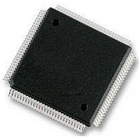
MC912D60CCPVE Freescale Semiconductor, MC912D60CCPVE Datasheet - Page 353

MC912D60CCPVE
Manufacturer Part Number
MC912D60CCPVE
Description
IC MCU 16BIT 112-LQFP
Manufacturer
Freescale Semiconductor
Series
HC12r
Datasheet
1.MC912D60ACFUE8.pdf
(460 pages)
Specifications of MC912D60CCPVE
Core Processor
CPU12
Core Size
16-Bit
Speed
8MHz
Connectivity
CAN, MI Bus, SCI, SPI
Peripherals
POR, PWM, WDT
Number Of I /o
68
Program Memory Size
60KB (60K x 8)
Program Memory Type
FLASH
Eeprom Size
1K x 8
Ram Size
2K x 8
Voltage - Supply (vcc/vdd)
4.5 V ~ 5.5 V
Data Converters
A/D 16x8/10b
Oscillator Type
Internal
Operating Temperature
-40°C ~ 85°C
Package / Case
112-LQFP
Processor Series
HC912D
Core
HC12
Data Bus Width
16 bit
Data Ram Size
2 KB
Interface Type
CAN, SCI, SPI
Maximum Clock Frequency
8 MHz
Number Of Programmable I/os
86
Maximum Operating Temperature
+ 85 C
Mounting Style
SMD/SMT
3rd Party Development Tools
EWHCS12
Minimum Operating Temperature
- 40 C
On-chip Adc
10 bit, 8 Channel
Lead Free Status / RoHS Status
Lead free / RoHS Compliant
Available stocks
Company
Part Number
Manufacturer
Quantity
Price
Company:
Part Number:
MC912D60CCPVE
Manufacturer:
FREESCAL
Quantity:
203
Company:
Part Number:
MC912D60CCPVE
Manufacturer:
Freescale Semiconductor
Quantity:
10 000
- Current page: 353 of 460
- Download datasheet (5Mb)
18.4.3 Sample and Hold Stage
18.4.4 Analog-to-Digital Converter Submodule
18.4.5 Clock Prescaler Function
MC68HC912D60A — Rev. 3.1
Freescale Semiconductor
A Sample and Hold (S/H) stage accepts the analog signal from the input
multiplexer and stores it as a capacitor charge on a storage node in the
module. The sample process uses a three stage approach:
This charge redistribution method eliminates the need for external
sample-and-hold circuitry.
The Analog-to-Digital (A/D) Machine uses a successive approximation
A/D architecture to perform analog to digital conversions. The resolution
of the A/D converter is selectable at either 8 or 10 bits. It functions by
comparing the stored analog sample potential with a series of digitally
generated analog potentials (using CDAC & RDAC arrays). By following
a binary search algorithm, the converter quickly locates the
approximating potential that is nearest to the sampled potential. At the
end of the conversion process (10 module clocks for 8-bit, 12 module
clocks for 10-bit), the Successive Approximation Register (SAR)
contains the nearest approximation to the sampled signal, given the
resolution of the A/D converter, and is transferred to the appropriate
results register in the selected format.
To keep the ATD module clock within the specified frequency range
(note: there is a minimum and maximum frequency), a clock prescaler
function is available. This function divides the system PCLK by a
1. The input signal is sampled onto a sample capacitor (for 2 module
2. The sample amplifier quickly charges the storage node with a
3. The input signal is connected directly to the storage node to
clocks).
copy of the sample capacitor potential (for 4 module clocks).
complete the sample for high accuracy (for 2, 4, 8 or 16 module
clocks). Longer sample times allow accurate measurement of
higher impedance sources.
Analog-to-Digital Converter
Analog-to-Digital Converter
Functional Description
Technical Data
353
Related parts for MC912D60CCPVE
Image
Part Number
Description
Manufacturer
Datasheet
Request
R
Part Number:
Description:
Manufacturer:
Freescale Semiconductor, Inc
Datasheet:
Part Number:
Description:
Manufacturer:
Freescale Semiconductor, Inc
Datasheet:
Part Number:
Description:
Manufacturer:
Freescale Semiconductor, Inc
Datasheet:
Part Number:
Description:
Manufacturer:
Freescale Semiconductor, Inc
Datasheet:
Part Number:
Description:
Manufacturer:
Freescale Semiconductor, Inc
Datasheet:
Part Number:
Description:
Manufacturer:
Freescale Semiconductor, Inc
Datasheet:
Part Number:
Description:
Manufacturer:
Freescale Semiconductor, Inc
Datasheet:
Part Number:
Description:
Manufacturer:
Freescale Semiconductor, Inc
Datasheet:
Part Number:
Description:
Manufacturer:
Freescale Semiconductor, Inc
Datasheet:
Part Number:
Description:
Manufacturer:
Freescale Semiconductor, Inc
Datasheet:
Part Number:
Description:
Manufacturer:
Freescale Semiconductor, Inc
Datasheet:
Part Number:
Description:
Manufacturer:
Freescale Semiconductor, Inc
Datasheet:
Part Number:
Description:
Manufacturer:
Freescale Semiconductor, Inc
Datasheet:
Part Number:
Description:
Manufacturer:
Freescale Semiconductor, Inc
Datasheet:
Part Number:
Description:
Manufacturer:
Freescale Semiconductor, Inc
Datasheet:


