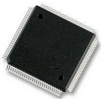
MC912D60CCPVE Freescale Semiconductor, MC912D60CCPVE Datasheet - Page 389

MC912D60CCPVE
Manufacturer Part Number
MC912D60CCPVE
Description
IC MCU 16BIT 112-LQFP
Manufacturer
Freescale Semiconductor
Series
HC12r
Datasheet
1.MC912D60ACFUE8.pdf
(460 pages)
Specifications of MC912D60CCPVE
Core Processor
CPU12
Core Size
16-Bit
Speed
8MHz
Connectivity
CAN, MI Bus, SCI, SPI
Peripherals
POR, PWM, WDT
Number Of I /o
68
Program Memory Size
60KB (60K x 8)
Program Memory Type
FLASH
Eeprom Size
1K x 8
Ram Size
2K x 8
Voltage - Supply (vcc/vdd)
4.5 V ~ 5.5 V
Data Converters
A/D 16x8/10b
Oscillator Type
Internal
Operating Temperature
-40°C ~ 85°C
Package / Case
112-LQFP
Processor Series
HC912D
Core
HC12
Data Bus Width
16 bit
Data Ram Size
2 KB
Interface Type
CAN, SCI, SPI
Maximum Clock Frequency
8 MHz
Number Of Programmable I/os
86
Maximum Operating Temperature
+ 85 C
Mounting Style
SMD/SMT
3rd Party Development Tools
EWHCS12
Minimum Operating Temperature
- 40 C
On-chip Adc
10 bit, 8 Channel
Lead Free Status / RoHS Status
Lead free / RoHS Compliant
Available stocks
Company
Part Number
Manufacturer
Quantity
Price
Company:
Part Number:
MC912D60CCPVE
Manufacturer:
FREESCAL
Quantity:
203
Company:
Part Number:
MC912D60CCPVE
Manufacturer:
Freescale Semiconductor
Quantity:
10 000
- Current page: 389 of 460
- Download datasheet (5Mb)
MC68HC912D60A — Rev. 3.1
Freescale Semiconductor
BDMACT — Background Mode Active Status
ENTAG — Tagging Enable
SDV — Shifter Data Valid
TRACE — Asserted by the TRACE1 command
BDMACT becomes set as active BDM mode is entered so that the
BDM firmware ROM is enabled and put into the map. BDMACT is
cleared by a carefully timed store instruction in the BDM firmware as
part of the exit sequence to return to user code and remove the BDM
memory from the map. This bit has 4 clock cycles write delay.
The user should be careful that the state of the BDMACT bit is not
unintentionally changed with the WRITE_NEXT firmware command.
If it is unintentionally changed from 1 to 0, it will cause a system
runaway because it would disable the BDM firmware ROM while the
CPU12 was executing BDM firmware. The following two commands
show how BDMACT may unintentionally get changed from 1 to 0.
WRITE_X with data $FEFE
WRITE_NEXT with data $C400
The first command writes the data $FEFE to the X index register. The
second command writes the data $C4 to the $FF00 INSTRUCTION
register and also writes the data $00 to the $FF01 STATUS register.
Set by the TAGGO command and cleared when BDM mode is
entered. The serial system is disabled and the tag function enabled
16 cycles after this bit is written.
Shows that valid data is in the serial interface shift register. Used by
the BDM firmware.
0 = BDM is not active. BDM ROM and registers are not in map.
1 = BDM is active and waiting for serial commands. BDM ROM and
0 = Tagging not enabled, or BDM active.
1 = Tagging active. BDM cannot process serial commands while
0 = No valid data. Shift operation is not complete.
1 = Valid Data. Shift operation is complete.
registers are in map
tagging is active.
Development Support
Background Debug Mode
Development Support
Technical Data
389
Related parts for MC912D60CCPVE
Image
Part Number
Description
Manufacturer
Datasheet
Request
R
Part Number:
Description:
Manufacturer:
Freescale Semiconductor, Inc
Datasheet:
Part Number:
Description:
Manufacturer:
Freescale Semiconductor, Inc
Datasheet:
Part Number:
Description:
Manufacturer:
Freescale Semiconductor, Inc
Datasheet:
Part Number:
Description:
Manufacturer:
Freescale Semiconductor, Inc
Datasheet:
Part Number:
Description:
Manufacturer:
Freescale Semiconductor, Inc
Datasheet:
Part Number:
Description:
Manufacturer:
Freescale Semiconductor, Inc
Datasheet:
Part Number:
Description:
Manufacturer:
Freescale Semiconductor, Inc
Datasheet:
Part Number:
Description:
Manufacturer:
Freescale Semiconductor, Inc
Datasheet:
Part Number:
Description:
Manufacturer:
Freescale Semiconductor, Inc
Datasheet:
Part Number:
Description:
Manufacturer:
Freescale Semiconductor, Inc
Datasheet:
Part Number:
Description:
Manufacturer:
Freescale Semiconductor, Inc
Datasheet:
Part Number:
Description:
Manufacturer:
Freescale Semiconductor, Inc
Datasheet:
Part Number:
Description:
Manufacturer:
Freescale Semiconductor, Inc
Datasheet:
Part Number:
Description:
Manufacturer:
Freescale Semiconductor, Inc
Datasheet:
Part Number:
Description:
Manufacturer:
Freescale Semiconductor, Inc
Datasheet:


