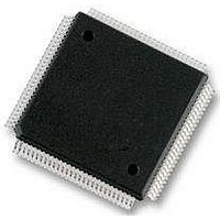
MC912D60CCPVE Freescale Semiconductor, MC912D60CCPVE Datasheet - Page 42

MC912D60CCPVE
Manufacturer Part Number
MC912D60CCPVE
Description
IC MCU 16BIT 112-LQFP
Manufacturer
Freescale Semiconductor
Series
HC12r
Datasheet
1.MC912D60ACFUE8.pdf
(460 pages)
Specifications of MC912D60CCPVE
Core Processor
CPU12
Core Size
16-Bit
Speed
8MHz
Connectivity
CAN, MI Bus, SCI, SPI
Peripherals
POR, PWM, WDT
Number Of I /o
68
Program Memory Size
60KB (60K x 8)
Program Memory Type
FLASH
Eeprom Size
1K x 8
Ram Size
2K x 8
Voltage - Supply (vcc/vdd)
4.5 V ~ 5.5 V
Data Converters
A/D 16x8/10b
Oscillator Type
Internal
Operating Temperature
-40°C ~ 85°C
Package / Case
112-LQFP
Processor Series
HC912D
Core
HC12
Data Bus Width
16 bit
Data Ram Size
2 KB
Interface Type
CAN, SCI, SPI
Maximum Clock Frequency
8 MHz
Number Of Programmable I/os
86
Maximum Operating Temperature
+ 85 C
Mounting Style
SMD/SMT
3rd Party Development Tools
EWHCS12
Minimum Operating Temperature
- 40 C
On-chip Adc
10 bit, 8 Channel
Lead Free Status / RoHS Status
Lead free / RoHS Compliant
Available stocks
Company
Part Number
Manufacturer
Quantity
Price
Company:
Part Number:
MC912D60CCPVE
Manufacturer:
FREESCAL
Quantity:
203
Company:
Part Number:
MC912D60CCPVE
Manufacturer:
Freescale Semiconductor
Quantity:
10 000
- Current page: 42 of 460
- Download datasheet (5Mb)
Pinout and Signal Descriptions
3.4 Power Supply Pins
3.4.1 Internal Power (V
3.4.2 External Power (V
3.4.3 V
3.4.4 Analog to Digital Reference Voltages (V
Technical Data
42
DDA
, V
SSA
MC68HC912D60A power and ground pins are described below and
summarized in
All power supply pins must be connected to appropriate supplies.
On no account must any pins be left floating.
Power is supplied to the MCU through V
transitions place high, short-duration current demands on the power
supply, use bypass capacitors with high-frequency characteristics and
place them as close to the MCU as possible. Bypass requirements
depend on how heavily the MCU pins are loaded.
External power and ground for I/O drivers. Because fast signal
transitions place high, short-duration current demands on the power
supply, use bypass capacitors with high-frequency characteristics and
place them as close to the MCU as possible. Bypass requirements
depend on how heavily the MCU pins are loaded.
Provides operating voltage and ground for the analog-to-digital
converter. This allows the supply voltage to the ATD to be bypassed
independently. Connecting V
used will not result in an increase of power consumption.
V
V
If the ATD modules are not used, leaving V
result in an increase of power consumption.
DD
RH0
RH1
DDX
) and Ground (V
, V
, V
) and Ground (V
RL0
RL1
Pinout and Signal Descriptions
: reference voltage high and low for ATD converter 0.
: reference voltage high and low for ATD converter 1.
Table
SS
3-1.
SSX
)
RH
)
, V
DDA
RL
)
to V
DD
DD
if the ATD modules are not
and V
RH
connected to V
MC68HC912D60A — Rev. 3.1
SS
Freescale Semiconductor
. Because fast signal
DD
will not
Related parts for MC912D60CCPVE
Image
Part Number
Description
Manufacturer
Datasheet
Request
R
Part Number:
Description:
Manufacturer:
Freescale Semiconductor, Inc
Datasheet:
Part Number:
Description:
Manufacturer:
Freescale Semiconductor, Inc
Datasheet:
Part Number:
Description:
Manufacturer:
Freescale Semiconductor, Inc
Datasheet:
Part Number:
Description:
Manufacturer:
Freescale Semiconductor, Inc
Datasheet:
Part Number:
Description:
Manufacturer:
Freescale Semiconductor, Inc
Datasheet:
Part Number:
Description:
Manufacturer:
Freescale Semiconductor, Inc
Datasheet:
Part Number:
Description:
Manufacturer:
Freescale Semiconductor, Inc
Datasheet:
Part Number:
Description:
Manufacturer:
Freescale Semiconductor, Inc
Datasheet:
Part Number:
Description:
Manufacturer:
Freescale Semiconductor, Inc
Datasheet:
Part Number:
Description:
Manufacturer:
Freescale Semiconductor, Inc
Datasheet:
Part Number:
Description:
Manufacturer:
Freescale Semiconductor, Inc
Datasheet:
Part Number:
Description:
Manufacturer:
Freescale Semiconductor, Inc
Datasheet:
Part Number:
Description:
Manufacturer:
Freescale Semiconductor, Inc
Datasheet:
Part Number:
Description:
Manufacturer:
Freescale Semiconductor, Inc
Datasheet:
Part Number:
Description:
Manufacturer:
Freescale Semiconductor, Inc
Datasheet:


