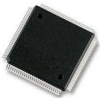
MC912D60CCPVE Freescale Semiconductor, MC912D60CCPVE Datasheet - Page 420

MC912D60CCPVE
Manufacturer Part Number
MC912D60CCPVE
Description
IC MCU 16BIT 112-LQFP
Manufacturer
Freescale Semiconductor
Series
HC12r
Datasheet
1.MC912D60ACFUE8.pdf
(460 pages)
Specifications of MC912D60CCPVE
Core Processor
CPU12
Core Size
16-Bit
Speed
8MHz
Connectivity
CAN, MI Bus, SCI, SPI
Peripherals
POR, PWM, WDT
Number Of I /o
68
Program Memory Size
60KB (60K x 8)
Program Memory Type
FLASH
Eeprom Size
1K x 8
Ram Size
2K x 8
Voltage - Supply (vcc/vdd)
4.5 V ~ 5.5 V
Data Converters
A/D 16x8/10b
Oscillator Type
Internal
Operating Temperature
-40°C ~ 85°C
Package / Case
112-LQFP
Processor Series
HC912D
Core
HC12
Data Bus Width
16 bit
Data Ram Size
2 KB
Interface Type
CAN, SCI, SPI
Maximum Clock Frequency
8 MHz
Number Of Programmable I/os
86
Maximum Operating Temperature
+ 85 C
Mounting Style
SMD/SMT
3rd Party Development Tools
EWHCS12
Minimum Operating Temperature
- 40 C
On-chip Adc
10 bit, 8 Channel
Lead Free Status / RoHS Status
Lead free / RoHS Compliant
Available stocks
Company
Part Number
Manufacturer
Quantity
Price
Company:
Part Number:
MC912D60CCPVE
Manufacturer:
FREESCAL
Quantity:
203
Company:
Part Number:
MC912D60CCPVE
Manufacturer:
Freescale Semiconductor
Quantity:
10 000
- Current page: 420 of 460
- Download datasheet (5Mb)
Electrical Specifications
Technical Data
420
Num
1. All timings are calculated for normal port drives.
2. Crystal input is required to be within 45% to 55% duty.
3. Reduced drive must be off to meet these timings.
4. Unequalled loading of pins will affect relative timing numbers.
5. This characteristic is affected by clock stretch.
6. Without TAG enabled.
10
11
12
13
14
15
16
17
18
19
20
21
22
23
24
25
26
1
2
3
5
7
8
9
Add N × t
Frequency of operation (ECLK frequency)
Cycle timet
Pulse width, E lowPW
Pulse width, E high
Address delay timet
Address valid time to ECLK riset
Multiplexed address hold timet
Address Hold to Data Valid
Data Hold to High Zt
Read data setup time
Read data hold time
Write data delay time
Write data hold time
Write data setup time
Read/write delay timet
Read/write valid time to E riset
Read/write hold time
Low strobe
Low strobe
Low strobe
Address access time
Access time from E rise
DBE delay from ECLK rise
DBE valid timet
DBE hold time from ECLK fall
cyc
where N = 0, 1, 2, or 3, depending on the number of clock stretches.
(6)
(6)
(6)
cyc
delay timet
valid time to E riset
hold time
= 1/f
DBE
V
DD
Table 20-14. Multiplexed Expansion Bus Timing
o
Characteristic
(5)
AD
= PW
= 5.0 Vdc ± 10%, V
DHZ
(5)
PW
(5)
EL
RWD
= t
t
t
ACCA
(5)
DSW
LSD
= t
= t
EH
EH
cyc
t
ACCE
(5)
= t
cyc
AD
= t
/4 + delay
− t
= t
t
= PW
= t
DBED
cyc
/2 + delay
MAH
− 20
RWV
cyc
DBED
cyc
cyc
= PW
AV
/4 + delay
LSV
/2 + delay
/4 + delay
(1), (2), (3), (4)
EH
= t
− t
= t
= PW
= PW
= PW
Electrical Specifications
AD
cyc
cyc
SS
− t
EH
/4 + delay
DDW
= 0 Vdc, T
/4 + delay
− t
EL
EL
− t
EL
DSR
DSR
− t
− t
− t
AD
RWD
LSD
A
= T
L
to T
H
, unless otherwise noted
Delay Symbol
−18
—
−4
−2
27
—
—
—
—
—
—
—
18
—
—
18
—
—
—
—
—
—
8
MC68HC912D60A — Rev. 3.1
PW
PW
t
t
t
t
t
t
t
t
t
t
t
t
AHDS
t
t
t
ACCA
ACCE
DBED
t
DBEH
t
t
t
DDW
DHW
DSW
RWD
RWV
RWH
t
MAH
DHR
t
DHZ
DSR
DBE
t
LSD
LSV
LSH
cyc
AD
f
AV
o
Freescale Semiconductor
EH
EL
0.004 8.0
0.125 250
Min
58
60
13
20
25
20
13
20
20
21
8
0
9
9
0
8 MHz
Max
50
30
47
49
49
50
35
39
10
MHz
Unit
µs
ns
ns
ns
ns
ns
ns
ns
ns
ns
ns
ns
ns
ns
ns
ns
ns
ns
ns
ns
ns
ns
ns
ns
Related parts for MC912D60CCPVE
Image
Part Number
Description
Manufacturer
Datasheet
Request
R
Part Number:
Description:
Manufacturer:
Freescale Semiconductor, Inc
Datasheet:
Part Number:
Description:
Manufacturer:
Freescale Semiconductor, Inc
Datasheet:
Part Number:
Description:
Manufacturer:
Freescale Semiconductor, Inc
Datasheet:
Part Number:
Description:
Manufacturer:
Freescale Semiconductor, Inc
Datasheet:
Part Number:
Description:
Manufacturer:
Freescale Semiconductor, Inc
Datasheet:
Part Number:
Description:
Manufacturer:
Freescale Semiconductor, Inc
Datasheet:
Part Number:
Description:
Manufacturer:
Freescale Semiconductor, Inc
Datasheet:
Part Number:
Description:
Manufacturer:
Freescale Semiconductor, Inc
Datasheet:
Part Number:
Description:
Manufacturer:
Freescale Semiconductor, Inc
Datasheet:
Part Number:
Description:
Manufacturer:
Freescale Semiconductor, Inc
Datasheet:
Part Number:
Description:
Manufacturer:
Freescale Semiconductor, Inc
Datasheet:
Part Number:
Description:
Manufacturer:
Freescale Semiconductor, Inc
Datasheet:
Part Number:
Description:
Manufacturer:
Freescale Semiconductor, Inc
Datasheet:
Part Number:
Description:
Manufacturer:
Freescale Semiconductor, Inc
Datasheet:
Part Number:
Description:
Manufacturer:
Freescale Semiconductor, Inc
Datasheet:


