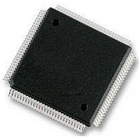
MC912D60CCPVE Freescale Semiconductor, MC912D60CCPVE Datasheet - Page 433

MC912D60CCPVE
Manufacturer Part Number
MC912D60CCPVE
Description
IC MCU 16BIT 112-LQFP
Manufacturer
Freescale Semiconductor
Series
HC12r
Datasheet
1.MC912D60ACFUE8.pdf
(460 pages)
Specifications of MC912D60CCPVE
Core Processor
CPU12
Core Size
16-Bit
Speed
8MHz
Connectivity
CAN, MI Bus, SCI, SPI
Peripherals
POR, PWM, WDT
Number Of I /o
68
Program Memory Size
60KB (60K x 8)
Program Memory Type
FLASH
Eeprom Size
1K x 8
Ram Size
2K x 8
Voltage - Supply (vcc/vdd)
4.5 V ~ 5.5 V
Data Converters
A/D 16x8/10b
Oscillator Type
Internal
Operating Temperature
-40°C ~ 85°C
Package / Case
112-LQFP
Processor Series
HC912D
Core
HC12
Data Bus Width
16 bit
Data Ram Size
2 KB
Interface Type
CAN, SCI, SPI
Maximum Clock Frequency
8 MHz
Number Of Programmable I/os
86
Maximum Operating Temperature
+ 85 C
Mounting Style
SMD/SMT
3rd Party Development Tools
EWHCS12
Minimum Operating Temperature
- 40 C
On-chip Adc
10 bit, 8 Channel
Lead Free Status / RoHS Status
Lead free / RoHS Compliant
Available stocks
Company
Part Number
Manufacturer
Quantity
Price
Company:
Part Number:
MC912D60CCPVE
Manufacturer:
FREESCAL
Quantity:
203
Company:
Part Number:
MC912D60CCPVE
Manufacturer:
Freescale Semiconductor
Quantity:
10 000
- Current page: 433 of 460
- Download datasheet (5Mb)
21.4 Printed Circuit Board Guidelines
MC68HC912D60A — Rev. 3.1
Freescale Semiconductor
Printed Circuit Boards (PCBs) are the board of choice for volume
applications. If designed correctly, a very low noise system can be built
on a PCB with consequently good EMI/EMC performances. If designed
incorrectly, PCBs can be extremely noisy and sensitive modules, and
the CGM could be disrupted. Some common sense rules can be used to
prevent such problems.
•
•
•
•
•
•
Use a ‘star’ style power routing plan as opposed to a ‘daisy chain’.
Route power and ground from a central location to each chip
individually, and use the widest trace practical (the more the chip
draws current, the wider the trace). NEVER place the MCU at the
end of a long string of serially connected chips.
When using PCB layout software, first direct the routing of the
power supply lines as well as the CGM wires (crystal oscillator and
PLL). Layout constraints must be then reported on the other
signals and not on these ‘hot’ nodes. Optimizing the ‘hot’ nodes at
the end of the routing process usually gives bad results.
Avoid notches in power traces. These notches not only add
resistance (and are not usually accounted for in simulations), but
they can also add unnecessary transmission line effects.
Avoid ground and power loops. This has been one of the most
violated guidelines of PCB layout. Loops are excellent noise
transmitters and can be easily avoided. When using multiple layer
PCBs, the power and ground plane concept works well but only
when strictly adhered to (do not compromise the ground plane by
cutting a hole in it and running signals on the ground plane layer).
Keep the spacing around via holes to a minimum (but not so small
as to add capacitive effects).
Be aware of the three dimensional capacitive effects of multi-
layered PCBs.
Bypass (decouple) the power supplies of all chips as close to the
chip as possible. Use one decoupling capacitor per power supply
pair (VDD/VSS, VDDX/VSSX...). Two capacitors with a ratio of
about 100 sometimes offer better performances over a broader
Appendix: CGM Practical Aspects
Appendix: CGM Practical Aspects
Printed Circuit Board Guidelines
Technical Data
433
Related parts for MC912D60CCPVE
Image
Part Number
Description
Manufacturer
Datasheet
Request
R
Part Number:
Description:
Manufacturer:
Freescale Semiconductor, Inc
Datasheet:
Part Number:
Description:
Manufacturer:
Freescale Semiconductor, Inc
Datasheet:
Part Number:
Description:
Manufacturer:
Freescale Semiconductor, Inc
Datasheet:
Part Number:
Description:
Manufacturer:
Freescale Semiconductor, Inc
Datasheet:
Part Number:
Description:
Manufacturer:
Freescale Semiconductor, Inc
Datasheet:
Part Number:
Description:
Manufacturer:
Freescale Semiconductor, Inc
Datasheet:
Part Number:
Description:
Manufacturer:
Freescale Semiconductor, Inc
Datasheet:
Part Number:
Description:
Manufacturer:
Freescale Semiconductor, Inc
Datasheet:
Part Number:
Description:
Manufacturer:
Freescale Semiconductor, Inc
Datasheet:
Part Number:
Description:
Manufacturer:
Freescale Semiconductor, Inc
Datasheet:
Part Number:
Description:
Manufacturer:
Freescale Semiconductor, Inc
Datasheet:
Part Number:
Description:
Manufacturer:
Freescale Semiconductor, Inc
Datasheet:
Part Number:
Description:
Manufacturer:
Freescale Semiconductor, Inc
Datasheet:
Part Number:
Description:
Manufacturer:
Freescale Semiconductor, Inc
Datasheet:
Part Number:
Description:
Manufacturer:
Freescale Semiconductor, Inc
Datasheet:


