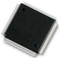
MC912D60CCPVE Freescale Semiconductor, MC912D60CCPVE Datasheet - Page 449

MC912D60CCPVE
Manufacturer Part Number
MC912D60CCPVE
Description
IC MCU 16BIT 112-LQFP
Manufacturer
Freescale Semiconductor
Series
HC12r
Datasheet
1.MC912D60ACFUE8.pdf
(460 pages)
Specifications of MC912D60CCPVE
Core Processor
CPU12
Core Size
16-Bit
Speed
8MHz
Connectivity
CAN, MI Bus, SCI, SPI
Peripherals
POR, PWM, WDT
Number Of I /o
68
Program Memory Size
60KB (60K x 8)
Program Memory Type
FLASH
Eeprom Size
1K x 8
Ram Size
2K x 8
Voltage - Supply (vcc/vdd)
4.5 V ~ 5.5 V
Data Converters
A/D 16x8/10b
Oscillator Type
Internal
Operating Temperature
-40°C ~ 85°C
Package / Case
112-LQFP
Processor Series
HC912D
Core
HC12
Data Bus Width
16 bit
Data Ram Size
2 KB
Interface Type
CAN, SCI, SPI
Maximum Clock Frequency
8 MHz
Number Of Programmable I/os
86
Maximum Operating Temperature
+ 85 C
Mounting Style
SMD/SMT
3rd Party Development Tools
EWHCS12
Minimum Operating Temperature
- 40 C
On-chip Adc
10 bit, 8 Channel
Lead Free Status / RoHS Status
Lead free / RoHS Compliant
Available stocks
Company
Part Number
Manufacturer
Quantity
Price
Company:
Part Number:
MC912D60CCPVE
Manufacturer:
FREESCAL
Quantity:
203
Company:
Part Number:
MC912D60CCPVE
Manufacturer:
Freescale Semiconductor
Quantity:
10 000
- Current page: 449 of 460
- Download datasheet (5Mb)
computer operating properly module (COP) — A counter module that resets the MCU if
condition code register (CCR) — An 8-bit register in the CPU that contains the interrupt mask
control bit — One bit of a register manipulated by software to control the operation of the
control unit — One of two major units of the CPU. The control unit contains logic functions that
COP — See "computer operating properly module (COP)."
CPU — See “central processor unit (CPU).”
CPU12 — The CPU of the MC68HC12 Family.
CPU clock — Bus clock select bits BCSP and BCSS in the clock select register (CLKSEL)
CPU cycles — A CPU cycle is one period of the internal bus clock, normally derived by dividing
CPU registers — Memory locations that are wired directly into the CPU logic instead of being
MC68HC912D60A — Rev. 3.1
Freescale Semiconductor
allowed to overflow.
bit and five bits that indicate the results of the instruction just executed.
module.
synchronize the machine and direct various operations. The control unit decodes
instructions and generates the internal control signals that perform the requested
operations. The outputs of the control unit drive the execution unit, which contains the
arithmetic logic unit (ALU), CPU registers, and bus interface.
determine which clock drives SYSCLK for the main system, including the CPU and buses.
When EXTALi drives the SYSCLK, the CPU or bus clock frequency (f
EXTALi frequency divided by 2.
a crystal oscillator source by two or more so the high and low times will be equal. The
length of time required to execute an instruction is measured in CPU clock cycles.
part of the addressable memory map. The CPU always has direct access to the
information in these registers. The CPU registers in an M68HC12 are:
•
•
•
•
•
•
•
A (8-bit accumulator)
B (8-bit accumulator)
–
IX (16-bit index register)
IY (16-bit index register)
SP (16-bit stack pointer)
PC (16-bit program counter)
CCR (8-bit condition code register)
D (16-bit accumulator formed by concatenation of accumulators A and B)
Glossary
o
) is equal to the
Technical Data
Glossary
449
Related parts for MC912D60CCPVE
Image
Part Number
Description
Manufacturer
Datasheet
Request
R
Part Number:
Description:
Manufacturer:
Freescale Semiconductor, Inc
Datasheet:
Part Number:
Description:
Manufacturer:
Freescale Semiconductor, Inc
Datasheet:
Part Number:
Description:
Manufacturer:
Freescale Semiconductor, Inc
Datasheet:
Part Number:
Description:
Manufacturer:
Freescale Semiconductor, Inc
Datasheet:
Part Number:
Description:
Manufacturer:
Freescale Semiconductor, Inc
Datasheet:
Part Number:
Description:
Manufacturer:
Freescale Semiconductor, Inc
Datasheet:
Part Number:
Description:
Manufacturer:
Freescale Semiconductor, Inc
Datasheet:
Part Number:
Description:
Manufacturer:
Freescale Semiconductor, Inc
Datasheet:
Part Number:
Description:
Manufacturer:
Freescale Semiconductor, Inc
Datasheet:
Part Number:
Description:
Manufacturer:
Freescale Semiconductor, Inc
Datasheet:
Part Number:
Description:
Manufacturer:
Freescale Semiconductor, Inc
Datasheet:
Part Number:
Description:
Manufacturer:
Freescale Semiconductor, Inc
Datasheet:
Part Number:
Description:
Manufacturer:
Freescale Semiconductor, Inc
Datasheet:
Part Number:
Description:
Manufacturer:
Freescale Semiconductor, Inc
Datasheet:
Part Number:
Description:
Manufacturer:
Freescale Semiconductor, Inc
Datasheet:


