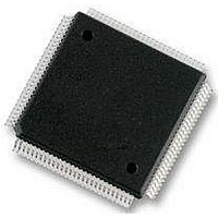
MC912D60CCPVE Freescale Semiconductor, MC912D60CCPVE Datasheet - Page 52

MC912D60CCPVE
Manufacturer Part Number
MC912D60CCPVE
Description
IC MCU 16BIT 112-LQFP
Manufacturer
Freescale Semiconductor
Series
HC12r
Datasheet
1.MC912D60ACFUE8.pdf
(460 pages)
Specifications of MC912D60CCPVE
Core Processor
CPU12
Core Size
16-Bit
Speed
8MHz
Connectivity
CAN, MI Bus, SCI, SPI
Peripherals
POR, PWM, WDT
Number Of I /o
68
Program Memory Size
60KB (60K x 8)
Program Memory Type
FLASH
Eeprom Size
1K x 8
Ram Size
2K x 8
Voltage - Supply (vcc/vdd)
4.5 V ~ 5.5 V
Data Converters
A/D 16x8/10b
Oscillator Type
Internal
Operating Temperature
-40°C ~ 85°C
Package / Case
112-LQFP
Processor Series
HC912D
Core
HC12
Data Bus Width
16 bit
Data Ram Size
2 KB
Interface Type
CAN, SCI, SPI
Maximum Clock Frequency
8 MHz
Number Of Programmable I/os
86
Maximum Operating Temperature
+ 85 C
Mounting Style
SMD/SMT
3rd Party Development Tools
EWHCS12
Minimum Operating Temperature
- 40 C
On-chip Adc
10 bit, 8 Channel
Lead Free Status / RoHS Status
Lead free / RoHS Compliant
Available stocks
Company
Part Number
Manufacturer
Quantity
Price
Company:
Part Number:
MC912D60CCPVE
Manufacturer:
FREESCAL
Quantity:
203
Company:
Part Number:
MC912D60CCPVE
Manufacturer:
Freescale Semiconductor
Quantity:
10 000
- Current page: 52 of 460
- Download datasheet (5Mb)
Pinout and Signal Descriptions
3.6 Port Signals
Technical Data
52
SDO/MOSI
1. In the 80-pin version PGUPD is connected internally to VDD
2. In the 80-pin version PHUPD is connected internally to VSS
Pin Name
SDI/MISO
KWG[6:0]
KWH[7:0]
AN1[7:0]
AN0[7:0]
IOC[7:0]
PGUPD
PHUPD
RxCAN
TxCAN
TEST
RxD1
RxD0
TxD1
TxD0
24 (KWH4
8 (KWG4
14–11,
80-pin
60–53
only)
only)
7–4
N/A
68
67
66
65
64
63
71
72
73
(1)
(2)
Pin Number
Table 3-2. MC68HC912D60A Signal Description Summary
84/82/80/78/
83/81/79/77/
9–11, 19–22
76/74/72/70
75/73/71/69
18–15, 7–4
112-pin
32–35,
The MC68HC912D60A incorporates eight ports which are used to
control and access the various device subsystems. When not used for
these purposes, port pins may be used for general-purpose I/O. In
addition to the pins described below, each port consists of a data register
49–52
104
105
94
93
97
13
41
92
91
90
89
Master out/slave in pin for serial peripheral interface
Master in/slave out pin for serial peripheral interface
SCI1 transmit pin
SCI1 receive pin
SCI0 transmit pin
SCI0 receive pin
Pins used for input capture and output compare in the timer and pulse
Analog inputs for the analog-to-digital conversion module 1
Analog inputs for the analog-to-digital conversion module 0
Used for factory test purposes. Do not connect in the application; may be
MSCAN transmit pin. Leave unconnected if MSCAN is not used.
MSCAN receive pin. Pin has internal pull-up; where msCAN module is not
Key wake-up and general purpose I/O; can cause an interrupt when an
Defines if I/O port resistive load is a pull-up or a pull-down, when enabled.
Key wake-up and general purpose I/O; can cause an interrupt when an
Defines if I/O port resistive load is a pull-up or a pull-down, when enabled.
accumulator subsystem.
bonded to 5.5 V max.
used, do not tie to VSS.
input transitions from high to low. On 80-pin QFP all 8 I/O should be
initialised.
input transitions from high to low. On 80-pin QFP all 8 I/O should be
initialised.
Pinout and Signal Descriptions
Description
MC68HC912D60A — Rev. 3.1
Freescale Semiconductor
Related parts for MC912D60CCPVE
Image
Part Number
Description
Manufacturer
Datasheet
Request
R
Part Number:
Description:
Manufacturer:
Freescale Semiconductor, Inc
Datasheet:
Part Number:
Description:
Manufacturer:
Freescale Semiconductor, Inc
Datasheet:
Part Number:
Description:
Manufacturer:
Freescale Semiconductor, Inc
Datasheet:
Part Number:
Description:
Manufacturer:
Freescale Semiconductor, Inc
Datasheet:
Part Number:
Description:
Manufacturer:
Freescale Semiconductor, Inc
Datasheet:
Part Number:
Description:
Manufacturer:
Freescale Semiconductor, Inc
Datasheet:
Part Number:
Description:
Manufacturer:
Freescale Semiconductor, Inc
Datasheet:
Part Number:
Description:
Manufacturer:
Freescale Semiconductor, Inc
Datasheet:
Part Number:
Description:
Manufacturer:
Freescale Semiconductor, Inc
Datasheet:
Part Number:
Description:
Manufacturer:
Freescale Semiconductor, Inc
Datasheet:
Part Number:
Description:
Manufacturer:
Freescale Semiconductor, Inc
Datasheet:
Part Number:
Description:
Manufacturer:
Freescale Semiconductor, Inc
Datasheet:
Part Number:
Description:
Manufacturer:
Freescale Semiconductor, Inc
Datasheet:
Part Number:
Description:
Manufacturer:
Freescale Semiconductor, Inc
Datasheet:
Part Number:
Description:
Manufacturer:
Freescale Semiconductor, Inc
Datasheet:


