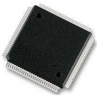
MC912D60CCPVE Freescale Semiconductor, MC912D60CCPVE Datasheet - Page 54

MC912D60CCPVE
Manufacturer Part Number
MC912D60CCPVE
Description
IC MCU 16BIT 112-LQFP
Manufacturer
Freescale Semiconductor
Series
HC12r
Datasheet
1.MC912D60ACFUE8.pdf
(460 pages)
Specifications of MC912D60CCPVE
Core Processor
CPU12
Core Size
16-Bit
Speed
8MHz
Connectivity
CAN, MI Bus, SCI, SPI
Peripherals
POR, PWM, WDT
Number Of I /o
68
Program Memory Size
60KB (60K x 8)
Program Memory Type
FLASH
Eeprom Size
1K x 8
Ram Size
2K x 8
Voltage - Supply (vcc/vdd)
4.5 V ~ 5.5 V
Data Converters
A/D 16x8/10b
Oscillator Type
Internal
Operating Temperature
-40°C ~ 85°C
Package / Case
112-LQFP
Processor Series
HC912D
Core
HC12
Data Bus Width
16 bit
Data Ram Size
2 KB
Interface Type
CAN, SCI, SPI
Maximum Clock Frequency
8 MHz
Number Of Programmable I/os
86
Maximum Operating Temperature
+ 85 C
Mounting Style
SMD/SMT
3rd Party Development Tools
EWHCS12
Minimum Operating Temperature
- 40 C
On-chip Adc
10 bit, 8 Channel
Lead Free Status / RoHS Status
Lead free / RoHS Compliant
Available stocks
Company
Part Number
Manufacturer
Quantity
Price
Company:
Part Number:
MC912D60CCPVE
Manufacturer:
FREESCAL
Quantity:
203
Company:
Part Number:
MC912D60CCPVE
Manufacturer:
Freescale Semiconductor
Quantity:
10 000
- Current page: 54 of 460
- Download datasheet (5Mb)
Pinout and Signal Descriptions
3.6.3 Port E
Technical Data
54
When the PUPB bit in the PUCR register is set, all port B input pins are
pulled-up internally by an active pull-up device. This bit has no effect if
the port is being used in expanded modes as the pull-ups are inactive.
Setting the RDPB bit in register RDRIV causes all port B outputs to have
reduced drive level. RDRIV can be written once after reset. RDRIV is not
in the address map in peripheral mode. Refer to
Input/Output.
Port E pins operate differently from port A and B pins. Port E pins are
used for bus control signals and interrupt service request signals. When
a pin is not used for one of these specific functions, it can be used as
general-purpose I/O. However, two of the pins (PE[1:0]) can only be
used for input, and the states of these pins can be read in the port data
register even when they are used for IRQ and XIRQ.
The PEAR register determines pin function, and register DDRE
determines whether each pin is an input or output when it is used for
general-purpose I/O. PEAR settings override DDRE settings. Because
PE[1:0] are input-only pins, only DDRE[7:2] have effect. Setting a bit in
the DDRE register makes the corresponding bit in port E an output;
clearing a bit in the DDRE register makes the corresponding bit in port E
an input. The default reset state of DDRE is all zeros.
When the PUPE bit in the PUCR register is set, PE7 and PE[3:0] are
pulled up by active devices.
Neither port E nor DDRE is in the map in peripheral mode; neither is in
the internal map in expanded modes with EME set.
Setting the RDPE bit in register RDRIV causes all port E outputs to have
reduced drive level. RDRIV can be written once after reset. RDRIV is not
in the address map in peripheral mode. Refer to
Input/Output.
Pinout and Signal Descriptions
MC68HC912D60A — Rev. 3.1
Bus Control and
Bus Control and
Freescale Semiconductor
Related parts for MC912D60CCPVE
Image
Part Number
Description
Manufacturer
Datasheet
Request
R
Part Number:
Description:
Manufacturer:
Freescale Semiconductor, Inc
Datasheet:
Part Number:
Description:
Manufacturer:
Freescale Semiconductor, Inc
Datasheet:
Part Number:
Description:
Manufacturer:
Freescale Semiconductor, Inc
Datasheet:
Part Number:
Description:
Manufacturer:
Freescale Semiconductor, Inc
Datasheet:
Part Number:
Description:
Manufacturer:
Freescale Semiconductor, Inc
Datasheet:
Part Number:
Description:
Manufacturer:
Freescale Semiconductor, Inc
Datasheet:
Part Number:
Description:
Manufacturer:
Freescale Semiconductor, Inc
Datasheet:
Part Number:
Description:
Manufacturer:
Freescale Semiconductor, Inc
Datasheet:
Part Number:
Description:
Manufacturer:
Freescale Semiconductor, Inc
Datasheet:
Part Number:
Description:
Manufacturer:
Freescale Semiconductor, Inc
Datasheet:
Part Number:
Description:
Manufacturer:
Freescale Semiconductor, Inc
Datasheet:
Part Number:
Description:
Manufacturer:
Freescale Semiconductor, Inc
Datasheet:
Part Number:
Description:
Manufacturer:
Freescale Semiconductor, Inc
Datasheet:
Part Number:
Description:
Manufacturer:
Freescale Semiconductor, Inc
Datasheet:
Part Number:
Description:
Manufacturer:
Freescale Semiconductor, Inc
Datasheet:


