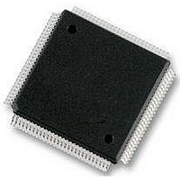
MC912D60CCPVE Freescale Semiconductor, MC912D60CCPVE Datasheet - Page 79

MC912D60CCPVE
Manufacturer Part Number
MC912D60CCPVE
Description
IC MCU 16BIT 112-LQFP
Manufacturer
Freescale Semiconductor
Series
HC12r
Datasheet
1.MC912D60ACFUE8.pdf
(460 pages)
Specifications of MC912D60CCPVE
Core Processor
CPU12
Core Size
16-Bit
Speed
8MHz
Connectivity
CAN, MI Bus, SCI, SPI
Peripherals
POR, PWM, WDT
Number Of I /o
68
Program Memory Size
60KB (60K x 8)
Program Memory Type
FLASH
Eeprom Size
1K x 8
Ram Size
2K x 8
Voltage - Supply (vcc/vdd)
4.5 V ~ 5.5 V
Data Converters
A/D 16x8/10b
Oscillator Type
Internal
Operating Temperature
-40°C ~ 85°C
Package / Case
112-LQFP
Processor Series
HC912D
Core
HC12
Data Bus Width
16 bit
Data Ram Size
2 KB
Interface Type
CAN, SCI, SPI
Maximum Clock Frequency
8 MHz
Number Of Programmable I/os
86
Maximum Operating Temperature
+ 85 C
Mounting Style
SMD/SMT
3rd Party Development Tools
EWHCS12
Minimum Operating Temperature
- 40 C
On-chip Adc
10 bit, 8 Channel
Lead Free Status / RoHS Status
Lead free / RoHS Compliant
Available stocks
Company
Part Number
Manufacturer
Quantity
Price
Company:
Part Number:
MC912D60CCPVE
Manufacturer:
FREESCAL
Quantity:
203
Company:
Part Number:
MC912D60CCPVE
Manufacturer:
Freescale Semiconductor
Quantity:
10 000
- Current page: 79 of 460
- Download datasheet (5Mb)
5.5.2 RAM Mapping
INITRM — Initialization of Internal RAM Position Register
MC68HC912D60A — Rev. 3.1
Freescale Semiconductor
RESET:
RAM15
Bit 7
0
RAM14
6
0
MMSWAI — Memory Mapping Interface Stop in Wait Control
The MC68HC912D60A has 2K byte of fully static RAM that is used for
storing instructions, variables, and temporary data during program
execution. After reset, RAM addressing begins at location $0000 but can
be assigned to any 2K byte boundary within the standard 64K byte
address space. Mapping of internal RAM is controlled by five bits in the
INITRM register.
After reset, the first 512 bytes of RAM have their access inhibited by the
presence of the register address space. After initial MCU configuration,
it is recommended to map the register space at location $0800.
RAM[15:11] — Internal RAM map position
This bit controls access to the memory mapping interface when in
Wait mode.
Normal modes: write anytime; special modes: write never. Read
anytime.
0 = Memory mapping interface continues to function during Wait
mode.
1 = Memory mapping interface access is shut down during Wait
mode.
These bits specify the upper five bits of the 16-bit RAM address.
Normal modes: write once; special modes: write anytime. Read
anytime.
Operating Modes and Resource Mapping
RAM13
5
0
RAM12
4
0
RAM11
3
0
Operating Modes and Resource Mapping
2
0
0
1
0
0
Internal Resource Mapping
Bit 0
0
0
Technical Data
$0010
79
Related parts for MC912D60CCPVE
Image
Part Number
Description
Manufacturer
Datasheet
Request
R
Part Number:
Description:
Manufacturer:
Freescale Semiconductor, Inc
Datasheet:
Part Number:
Description:
Manufacturer:
Freescale Semiconductor, Inc
Datasheet:
Part Number:
Description:
Manufacturer:
Freescale Semiconductor, Inc
Datasheet:
Part Number:
Description:
Manufacturer:
Freescale Semiconductor, Inc
Datasheet:
Part Number:
Description:
Manufacturer:
Freescale Semiconductor, Inc
Datasheet:
Part Number:
Description:
Manufacturer:
Freescale Semiconductor, Inc
Datasheet:
Part Number:
Description:
Manufacturer:
Freescale Semiconductor, Inc
Datasheet:
Part Number:
Description:
Manufacturer:
Freescale Semiconductor, Inc
Datasheet:
Part Number:
Description:
Manufacturer:
Freescale Semiconductor, Inc
Datasheet:
Part Number:
Description:
Manufacturer:
Freescale Semiconductor, Inc
Datasheet:
Part Number:
Description:
Manufacturer:
Freescale Semiconductor, Inc
Datasheet:
Part Number:
Description:
Manufacturer:
Freescale Semiconductor, Inc
Datasheet:
Part Number:
Description:
Manufacturer:
Freescale Semiconductor, Inc
Datasheet:
Part Number:
Description:
Manufacturer:
Freescale Semiconductor, Inc
Datasheet:
Part Number:
Description:
Manufacturer:
Freescale Semiconductor, Inc
Datasheet:


