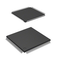
HD64F2166VTE33 Renesas Electronics America, HD64F2166VTE33 Datasheet - Page 633

HD64F2166VTE33
Manufacturer Part Number
HD64F2166VTE33
Description
IC H8S MCU FLASH 512K 144-TQFP
Manufacturer
Renesas Electronics America
Series
H8® H8S/2100r
Specifications of HD64F2166VTE33
Core Processor
H8S/2000
Core Size
16-Bit
Speed
33MHz
Connectivity
I²C, IrDA, LPC, SCI, SmartCard
Peripherals
POR, PWM, WDT
Number Of I /o
106
Program Memory Size
512KB (512K x 8)
Program Memory Type
FLASH
Ram Size
40K x 8
Voltage - Supply (vcc/vdd)
3 V ~ 3.6 V
Data Converters
A/D 8x10b; D/A 2x8b
Oscillator Type
Internal
Operating Temperature
-20°C ~ 75°C
Package / Case
144-TQFP, 144-VQFP
Lead Free Status / RoHS Status
Contains lead / RoHS non-compliant
Eeprom Size
-
Available stocks
Company
Part Number
Manufacturer
Quantity
Price
Company:
Part Number:
HD64F2166VTE33V
Manufacturer:
Renesas
Quantity:
200
Company:
Part Number:
HD64F2166VTE33V
Manufacturer:
ON
Quantity:
75
Part Number:
HD64F2166VTE33V
Manufacturer:
RENESAS/瑞萨
Quantity:
20 000
- Current page: 633 of 876
- Download datasheet (5Mb)
17.3
The D/A converter has the following registers.
• D/A data register 0 (DADR0)
• D/A data register 1 (DADR1)
• D/A control register (DACR)
17.3.1
DADR0 and DADR1 are 8-bit readable/writable registers that store data for D/A conversion.
When analog output is permitted, D/A data register contents are converted and output to analog
output pins.
17.3.2
DACR controls D/A converter operation.
Bit
7
6
5
4 to 0
Bit Name Initial Value
DAOE1
DAOE0
DAE
Register Descriptions
D/A Data Registers 0 and 1 (DADR0, DADR1)
D/A Control Register (DACR)
0
0
0
All 1
R/W
R/W
R/W
R
R/W
Description
D/A Output Enable 1
Controls D/A conversion and analog output.
0: Analog output DA1 is disabled
1: D/A conversion for channel 1 and analog output DA1
D/A Output Enable 0
Controls D/A conversion and analog output.
0: Analog output DA0 is disabled
1: D/A conversion for channel 0 and analog output DA0
D/A Enable
Controls D/A conversion in conjunction with the DAOE0
and DAOE1 bits. When the DAE bit is cleared to 0, D/A
conversion for channels 0 and 1 are controlled
individually. When the DAE bit is set to 1, D/A conversion
for channels 0 and 1 are controlled as one. Conversion
result output is controlled by the DAOE0 and DAOE1
bits. For details, see table 17.2 below.
Reserved
The initial value should not be changed.
are enabled
are enabled
Rev. 3.00, 03/04, page 591 of 830
Related parts for HD64F2166VTE33
Image
Part Number
Description
Manufacturer
Datasheet
Request
R

Part Number:
Description:
KIT STARTER FOR M16C/29
Manufacturer:
Renesas Electronics America
Datasheet:

Part Number:
Description:
KIT STARTER FOR R8C/2D
Manufacturer:
Renesas Electronics America
Datasheet:

Part Number:
Description:
R0K33062P STARTER KIT
Manufacturer:
Renesas Electronics America
Datasheet:

Part Number:
Description:
KIT STARTER FOR R8C/23 E8A
Manufacturer:
Renesas Electronics America
Datasheet:

Part Number:
Description:
KIT STARTER FOR R8C/25
Manufacturer:
Renesas Electronics America
Datasheet:

Part Number:
Description:
KIT STARTER H8S2456 SHARPE DSPLY
Manufacturer:
Renesas Electronics America
Datasheet:

Part Number:
Description:
KIT STARTER FOR R8C38C
Manufacturer:
Renesas Electronics America
Datasheet:

Part Number:
Description:
KIT STARTER FOR R8C35C
Manufacturer:
Renesas Electronics America
Datasheet:

Part Number:
Description:
KIT STARTER FOR R8CL3AC+LCD APPS
Manufacturer:
Renesas Electronics America
Datasheet:

Part Number:
Description:
KIT STARTER FOR RX610
Manufacturer:
Renesas Electronics America
Datasheet:

Part Number:
Description:
KIT STARTER FOR R32C/118
Manufacturer:
Renesas Electronics America
Datasheet:

Part Number:
Description:
KIT DEV RSK-R8C/26-29
Manufacturer:
Renesas Electronics America
Datasheet:

Part Number:
Description:
KIT STARTER FOR SH7124
Manufacturer:
Renesas Electronics America
Datasheet:

Part Number:
Description:
KIT STARTER FOR H8SX/1622
Manufacturer:
Renesas Electronics America
Datasheet:

Part Number:
Description:
KIT DEV FOR SH7203
Manufacturer:
Renesas Electronics America
Datasheet:


