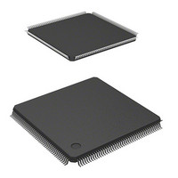
DS72011RB120FPV Renesas Electronics America, DS72011RB120FPV Datasheet - Page 1017

DS72011RB120FPV
Manufacturer Part Number
DS72011RB120FPV
Description
IC SH7201 MPU ROMLESS 176LQFP
Manufacturer
Renesas Electronics America
Series
SuperH® SH7200r
Datasheet
1.R0K572011S000BE.pdf
(1222 pages)
Specifications of DS72011RB120FPV
Core Size
32-Bit
Core Processor
SH-2A
Speed
120MHz
Connectivity
CAN, EBI/EMI, FIFO, I²C, SCI, Serial Sound
Peripherals
DMA, POR, PWM, WDT
Number Of I /o
104
Program Memory Type
ROMless
Ram Size
32K x 8
Voltage - Supply (vcc/vdd)
3 V ~ 3.6 V
Data Converters
A/D 8x10b; D/A 2x8b
Oscillator Type
Internal
Operating Temperature
-20°C ~ 70°C
Package / Case
176-LQFP
No. Of I/o's
109
Ram Memory Size
32KB
Cpu Speed
120MHz
Digital Ic Case Style
LQFP
Supply Voltage Range
3V To 3.6V
Operating Temperature Range
-20°C To +70°C
Embedded Interface Type
I2C, SSI
Rohs Compliant
Yes
Lead Free Status / RoHS Status
Lead free / RoHS Compliant
For Use With
R0K572011S000BE - KIT STARTER FOR SH7201HS0005KCU11H - EMULATOR E10A-USB H8S(X),SH2(A)
Eeprom Size
-
Program Memory Size
-
Lead Free Status / RoHS Status
Lead free / RoHS Compliant, Lead free / RoHS Compliant
Available stocks
Company
Part Number
Manufacturer
Quantity
Price
Company:
Part Number:
DS72011RB120FPV
Manufacturer:
Renesas Electronics America
Quantity:
10 000
- Current page: 1017 of 1222
- Download datasheet (8Mb)
SH7201 Group
This LSI has an on-chip RAM module that achieves high-speed access and can store instructions
or data.
On-chip RAM operation and write access to the RAM can be enabled or disabled through the
RAM enable bits and RAM write enable bits.
24.1
• Pages
• Memory map
Table 24.1 On-Chip RAM Address Spaces
• Ports
• Priority
R01UH0026EJ0300 Rev. 3.00
Sep 24, 2010
Page
Page 0
Page 1
Two pages (pages 0 and 1) are provided.
The on-chip RAM is located in the address spaces shown in table 24.1.
Each page has two independent read and write ports and is connected to the internal bus (I
bus), CPU instruction fetch bus (F bus), and CPU memory access bus (M bus). (Note that the F
bus is connected only to the read ports.)
The F bus and M bus are used for access by the CPU, and the I bus is used for access by the
DMAC via the internal DMA write bus/internal DMA read bus and bus bridge.
When requests for access to the same page from different buses coincide, the access is
processed in priority order. The priority is I bus > M bus > F bus.
Features
Section 24 On-Chip RAM
Address
H'FFF80000 to H'FFF83FFF
H'FFF84000 to H'FFF87FFF
Section 24 On-Chip RAM
Page 989 of 1190
Related parts for DS72011RB120FPV
Image
Part Number
Description
Manufacturer
Datasheet
Request
R

Part Number:
Description:
KIT STARTER FOR M16C/29
Manufacturer:
Renesas Electronics America
Datasheet:

Part Number:
Description:
KIT STARTER FOR R8C/2D
Manufacturer:
Renesas Electronics America
Datasheet:

Part Number:
Description:
R0K33062P STARTER KIT
Manufacturer:
Renesas Electronics America
Datasheet:

Part Number:
Description:
KIT STARTER FOR R8C/23 E8A
Manufacturer:
Renesas Electronics America
Datasheet:

Part Number:
Description:
KIT STARTER FOR R8C/25
Manufacturer:
Renesas Electronics America
Datasheet:

Part Number:
Description:
KIT STARTER H8S2456 SHARPE DSPLY
Manufacturer:
Renesas Electronics America
Datasheet:

Part Number:
Description:
KIT STARTER FOR R8C38C
Manufacturer:
Renesas Electronics America
Datasheet:

Part Number:
Description:
KIT STARTER FOR R8C35C
Manufacturer:
Renesas Electronics America
Datasheet:

Part Number:
Description:
KIT STARTER FOR R8CL3AC+LCD APPS
Manufacturer:
Renesas Electronics America
Datasheet:

Part Number:
Description:
KIT STARTER FOR RX610
Manufacturer:
Renesas Electronics America
Datasheet:

Part Number:
Description:
KIT STARTER FOR R32C/118
Manufacturer:
Renesas Electronics America
Datasheet:

Part Number:
Description:
KIT DEV RSK-R8C/26-29
Manufacturer:
Renesas Electronics America
Datasheet:

Part Number:
Description:
KIT STARTER FOR SH7124
Manufacturer:
Renesas Electronics America
Datasheet:

Part Number:
Description:
KIT STARTER FOR H8SX/1622
Manufacturer:
Renesas Electronics America
Datasheet:

Part Number:
Description:
KIT DEV FOR SH7203
Manufacturer:
Renesas Electronics America
Datasheet:


