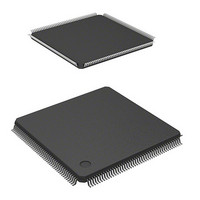
DS72011RB120FPV Renesas Electronics America, DS72011RB120FPV Datasheet - Page 1208

DS72011RB120FPV
Manufacturer Part Number
DS72011RB120FPV
Description
IC SH7201 MPU ROMLESS 176LQFP
Manufacturer
Renesas Electronics America
Series
SuperH® SH7200r
Datasheet
1.R0K572011S000BE.pdf
(1222 pages)
Specifications of DS72011RB120FPV
Core Size
32-Bit
Core Processor
SH-2A
Speed
120MHz
Connectivity
CAN, EBI/EMI, FIFO, I²C, SCI, Serial Sound
Peripherals
DMA, POR, PWM, WDT
Number Of I /o
104
Program Memory Type
ROMless
Ram Size
32K x 8
Voltage - Supply (vcc/vdd)
3 V ~ 3.6 V
Data Converters
A/D 8x10b; D/A 2x8b
Oscillator Type
Internal
Operating Temperature
-20°C ~ 70°C
Package / Case
176-LQFP
No. Of I/o's
109
Ram Memory Size
32KB
Cpu Speed
120MHz
Digital Ic Case Style
LQFP
Supply Voltage Range
3V To 3.6V
Operating Temperature Range
-20°C To +70°C
Embedded Interface Type
I2C, SSI
Rohs Compliant
Yes
Lead Free Status / RoHS Status
Lead free / RoHS Compliant
For Use With
R0K572011S000BE - KIT STARTER FOR SH7201HS0005KCU11H - EMULATOR E10A-USB H8S(X),SH2(A)
Eeprom Size
-
Program Memory Size
-
Lead Free Status / RoHS Status
Lead free / RoHS Compliant, Lead free / RoHS Compliant
Available stocks
Company
Part Number
Manufacturer
Quantity
Price
Company:
Part Number:
DS72011RB120FPV
Manufacturer:
Renesas Electronics America
Quantity:
10 000
- Current page: 1208 of 1222
- Download datasheet (8Mb)
Main Revisions for This Edition
Page 1180 of 1190
Item
29.3.3 Bus Timing
Figure 29.11 External Address
Space: Basic Bus Timing (Page
Read Access, Normal Access
Compatible Mode , Read Cycle
Wait = 2, Page Read Cycle Wait =
2, CS Assert Wait = 1, RD Assert
Wait = 1, Read CS Delay Cycles =
1)
Figure 29.12 External Address
Space: Basic Bus Timing (Page
Read Access, External Read Data
Continuous Assert Mode, Read
Cycle Wait = 2, Page Read Cycle
Wait = 1, CS Assert Wait = 1, RD
Assert Wait = 1, Read CS Delay
Cycles = 1)
Figure 29.13 External Address
Space: Basic Bus Timing (Page
Write Access, Write Cycle Wait =
2, CS Assert Wait = 1, WR Assert
Wait = 1, Write Data Output Delay
Cycles = 1, Other Wait Settings =
0)
Figure 29.14 External Address
Space: Timing with External Wait
(Page Read Access to 16-Bit
Width Channel, External Read
Data Continuous Assert Mode,
Read Cycle Wait = 3, Page Read
Cycle Wait = 3, Other Wait
Settings = 0, External Wait Cycles
= 2)
Figure 29.15 Single Read Bus
Timing for SDRAM Space (DCL =
2 (Two Cycles), DRCD = 1 (Two
Cycles), DPCG = 1 (Two Cycles))
Page
1126
1126
1127
1128
1129
Revision (See Manual for Details)
Figure title amended
Figure and figure title amended
CKIO
A27 to A0
BC3 to BC0
CSn
RD
D31 to D0
Figure and figure title amended
Figure and figure title amended
BC3 to BC0 → BC1, BC0
D31 to D0 → D15 to D0
Figure title amended
CKIO
t
t
Tw1
AD1
BCD
Tw1
Tw2
t
RSD
Tw2
Tend
Tend (Trd)
t
RDS1
Tdw1
t
t
BCD
AD1
Tpw1
Tpw1
t
RDH1
Tend (Trd)
t
RDS1
Tend
t
AD1
Tpw1
Tdw1
t
RDH1
Tend (Trd)
Tpw1
t
RDS1
R01UH0026EJ0300 Rev. 3.00
t
Tend
BCD
t
AD1
Tpw1
t
RDH1
Tdw1
Tend (Trd)
t
RDS1
Tpw1
t
BCD
t
t
AD1
RSD
Tn1
t
t
Tend
SH7201 Group
RDH1
RDH1
t
Sep 24, 2010
CSD1
Tdw1 (Tn1)
Ts
t
t
BCD
AD1
Related parts for DS72011RB120FPV
Image
Part Number
Description
Manufacturer
Datasheet
Request
R

Part Number:
Description:
KIT STARTER FOR M16C/29
Manufacturer:
Renesas Electronics America
Datasheet:

Part Number:
Description:
KIT STARTER FOR R8C/2D
Manufacturer:
Renesas Electronics America
Datasheet:

Part Number:
Description:
R0K33062P STARTER KIT
Manufacturer:
Renesas Electronics America
Datasheet:

Part Number:
Description:
KIT STARTER FOR R8C/23 E8A
Manufacturer:
Renesas Electronics America
Datasheet:

Part Number:
Description:
KIT STARTER FOR R8C/25
Manufacturer:
Renesas Electronics America
Datasheet:

Part Number:
Description:
KIT STARTER H8S2456 SHARPE DSPLY
Manufacturer:
Renesas Electronics America
Datasheet:

Part Number:
Description:
KIT STARTER FOR R8C38C
Manufacturer:
Renesas Electronics America
Datasheet:

Part Number:
Description:
KIT STARTER FOR R8C35C
Manufacturer:
Renesas Electronics America
Datasheet:

Part Number:
Description:
KIT STARTER FOR R8CL3AC+LCD APPS
Manufacturer:
Renesas Electronics America
Datasheet:

Part Number:
Description:
KIT STARTER FOR RX610
Manufacturer:
Renesas Electronics America
Datasheet:

Part Number:
Description:
KIT STARTER FOR R32C/118
Manufacturer:
Renesas Electronics America
Datasheet:

Part Number:
Description:
KIT DEV RSK-R8C/26-29
Manufacturer:
Renesas Electronics America
Datasheet:

Part Number:
Description:
KIT STARTER FOR SH7124
Manufacturer:
Renesas Electronics America
Datasheet:

Part Number:
Description:
KIT STARTER FOR H8SX/1622
Manufacturer:
Renesas Electronics America
Datasheet:

Part Number:
Description:
KIT DEV FOR SH7203
Manufacturer:
Renesas Electronics America
Datasheet:


