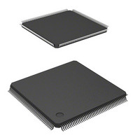
DS72011RB120FPV Renesas Electronics America, DS72011RB120FPV Datasheet - Page 922

DS72011RB120FPV
Manufacturer Part Number
DS72011RB120FPV
Description
IC SH7201 MPU ROMLESS 176LQFP
Manufacturer
Renesas Electronics America
Series
SuperH® SH7200r
Datasheet
1.R0K572011S000BE.pdf
(1222 pages)
Specifications of DS72011RB120FPV
Core Size
32-Bit
Core Processor
SH-2A
Speed
120MHz
Connectivity
CAN, EBI/EMI, FIFO, I²C, SCI, Serial Sound
Peripherals
DMA, POR, PWM, WDT
Number Of I /o
104
Program Memory Type
ROMless
Ram Size
32K x 8
Voltage - Supply (vcc/vdd)
3 V ~ 3.6 V
Data Converters
A/D 8x10b; D/A 2x8b
Oscillator Type
Internal
Operating Temperature
-20°C ~ 70°C
Package / Case
176-LQFP
No. Of I/o's
109
Ram Memory Size
32KB
Cpu Speed
120MHz
Digital Ic Case Style
LQFP
Supply Voltage Range
3V To 3.6V
Operating Temperature Range
-20°C To +70°C
Embedded Interface Type
I2C, SSI
Rohs Compliant
Yes
Lead Free Status / RoHS Status
Lead free / RoHS Compliant
For Use With
R0K572011S000BE - KIT STARTER FOR SH7201HS0005KCU11H - EMULATOR E10A-USB H8S(X),SH2(A)
Eeprom Size
-
Program Memory Size
-
Lead Free Status / RoHS Status
Lead free / RoHS Compliant, Lead free / RoHS Compliant
Available stocks
Company
Part Number
Manufacturer
Quantity
Price
Company:
Part Number:
DS72011RB120FPV
Manufacturer:
Renesas Electronics America
Quantity:
10 000
- Current page: 922 of 1222
- Download datasheet (8Mb)
Section 20 A/D Converter (ADC)
20.4.4
The A/D converter can be independently activated by an A/D conversion request from the external
trigger, MTU2, or TMR. To activate the A/D converter by the external trigger, MTU2, or TMR,
set the A/D trigger enable bits (TRGS[3:0]). After this bit setting has been made, the ADST bit is
automatically set to 1 and A/D conversion is started when an A/D conversion request from the
external trigger, MTU2, or TMR occurs. The channel combination is determined by the CH[2:0]
bits in ADCSR. The timing from setting of the ADST bit until the start of A/D conversion is the
same as when 1 is written to the ADST bit by software.
20.4.5
The A/D converter has a built-in sample-and-hold circuit. The A/D converter samples the analog
input at the A/D conversion start delay time (t
starts conversion. Figure 20.5 shows the A/D conversion timing. Table 20.4 indicates the A/D
conversion time.
As indicated in figure 20.5, the A/D conversion time (t
time(t
conversion time therefore varies within the ranges indicated in table 20.4.
In multi mode and scan mode, the values given in table 20.4 apply to the first conversion. In the
second and subsequent conversions, time is the values given in table 20.5.
Page 894 of 1190
SPL
). The length of t
A/D Converter Activation by External Trigger, MTU2, or TMR
Input Sampling and A/D Conversion Time
D
varies depending on the timing of the write access to ADCSR. The total
D
) after the ADST bit in ADCSR is set to 1, then
CONV
) includes t
D
and the input sampling
R01UH0026EJ0300 Rev. 3.00
SH7201 Group
Sep 24, 2010
Related parts for DS72011RB120FPV
Image
Part Number
Description
Manufacturer
Datasheet
Request
R

Part Number:
Description:
KIT STARTER FOR M16C/29
Manufacturer:
Renesas Electronics America
Datasheet:

Part Number:
Description:
KIT STARTER FOR R8C/2D
Manufacturer:
Renesas Electronics America
Datasheet:

Part Number:
Description:
R0K33062P STARTER KIT
Manufacturer:
Renesas Electronics America
Datasheet:

Part Number:
Description:
KIT STARTER FOR R8C/23 E8A
Manufacturer:
Renesas Electronics America
Datasheet:

Part Number:
Description:
KIT STARTER FOR R8C/25
Manufacturer:
Renesas Electronics America
Datasheet:

Part Number:
Description:
KIT STARTER H8S2456 SHARPE DSPLY
Manufacturer:
Renesas Electronics America
Datasheet:

Part Number:
Description:
KIT STARTER FOR R8C38C
Manufacturer:
Renesas Electronics America
Datasheet:

Part Number:
Description:
KIT STARTER FOR R8C35C
Manufacturer:
Renesas Electronics America
Datasheet:

Part Number:
Description:
KIT STARTER FOR R8CL3AC+LCD APPS
Manufacturer:
Renesas Electronics America
Datasheet:

Part Number:
Description:
KIT STARTER FOR RX610
Manufacturer:
Renesas Electronics America
Datasheet:

Part Number:
Description:
KIT STARTER FOR R32C/118
Manufacturer:
Renesas Electronics America
Datasheet:

Part Number:
Description:
KIT DEV RSK-R8C/26-29
Manufacturer:
Renesas Electronics America
Datasheet:

Part Number:
Description:
KIT STARTER FOR SH7124
Manufacturer:
Renesas Electronics America
Datasheet:

Part Number:
Description:
KIT STARTER FOR H8SX/1622
Manufacturer:
Renesas Electronics America
Datasheet:

Part Number:
Description:
KIT DEV FOR SH7203
Manufacturer:
Renesas Electronics America
Datasheet:


