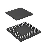
HD6417720BP133BV Renesas Electronics America, HD6417720BP133BV Datasheet - Page 243

HD6417720BP133BV
Manufacturer Part Number
HD6417720BP133BV
Description
SH3-DSP, WITH USB AND LCDC, PB-F
Manufacturer
Renesas Electronics America
Series
SuperH® SH7700r
Datasheet
1.R8A77210C133BAV.pdf
(1478 pages)
Specifications of HD6417720BP133BV
Core Processor
SH-3 DSP
Core Size
32-Bit
Speed
133MHz
Connectivity
FIFO, I²C, IrDA, MMC, SCI, SD, SIO, SIM, USB
Peripherals
DMA, LCD, POR, WDT
Number Of I /o
117
Program Memory Type
ROMless
Ram Size
16K x 8
Voltage - Supply (vcc/vdd)
1.4 V ~ 1.6 V
Data Converters
A/D 4x10b; D/A 2x8b
Oscillator Type
Internal
Operating Temperature
-20°C ~ 75°C
Package / Case
256-BGA
Lead Free Status / RoHS Status
Lead free / RoHS Compliant
Eeprom Size
-
Program Memory Size
-
- Current page: 243 of 1478
- Download datasheet (10Mb)
SH7720 Group, SH7721 Group
4.4.2
There are three kinds of MMU software management, as follows.
1. MMU register setting
2. TLB entry recording, deletion, and reading
3. MMU exception processing
When single virtual memory mode is used, it is possible to create a state in which physical
memory access is enabled in the privileged mode only by clearing the share status bit (SH) to 0 to
specify recording of all TLB entries. This strengthens inter-process memory protection, and
enables special access levels to be created in the privileged mode only.
Recording a 1- or 4- kbyte page TLB entry may result in a synonym problem. See section 4.4.4,
Avoiding Synonym Problems.
4.4.3
The load TLB instruction (LDTLB) is used to record TLB entries. When the IX bit in MMUCR is
0, the LDTLB instruction changes the TLB entry in the way specified by the RC bit in MMUCR
to the value specified by PTEH and PTEL, using VPN bits 16 to 12 specified in PTEH as the
index number. When the IX bit in MMUCR is 1, the EX-OR of VPN bits 16 to 12 specified in
PTEH and ASID bits 4 to 0 in PTEH are used as the index number.
R01UH0083EJ0400 Rev. 4.00
Sep 21, 2010
MMUCR setting, in particular, should be performed in areas P1 and P2 for which address
translation is not performed. Also, since SV and IX bit changes constitute address translation
system changes, in this case, TLB flushing should be performed by simultaneously writing 1 to
the TF bit also. Since MMU exceptions are not generated in the MMU disabled state with the
AT bit cleared to 0, use in the disabled state must be avoided with software that does not use
the MMU.
TLB entry recording can be done in two ways by using the LDTLB instruction, or by writing
directly to the memory-mapped TLB. For TLB entry deletion and reading, the memory
allocation TLB can be accessed. See section 4.4.3, MMU Instruction (LDTLB), for details of
the LDTLB instruction, and section 4.6, Memory-Mapped TLB, for details of the memory-
mapped TLB.
When an MMU exception is generated, it is handled on the basis of information set from the
hardware side. See section 4.5, MMU Exceptions, for details.
MMU Software Management
MMU Instruction (LDTLB)
Section 4 Memory Management Unit (MMU)
Page 183 of 1414
Related parts for HD6417720BP133BV
Image
Part Number
Description
Manufacturer
Datasheet
Request
R

Part Number:
Description:
KIT STARTER FOR M16C/29
Manufacturer:
Renesas Electronics America
Datasheet:

Part Number:
Description:
KIT STARTER FOR R8C/2D
Manufacturer:
Renesas Electronics America
Datasheet:

Part Number:
Description:
R0K33062P STARTER KIT
Manufacturer:
Renesas Electronics America
Datasheet:

Part Number:
Description:
KIT STARTER FOR R8C/23 E8A
Manufacturer:
Renesas Electronics America
Datasheet:

Part Number:
Description:
KIT STARTER FOR R8C/25
Manufacturer:
Renesas Electronics America
Datasheet:

Part Number:
Description:
KIT STARTER H8S2456 SHARPE DSPLY
Manufacturer:
Renesas Electronics America
Datasheet:

Part Number:
Description:
KIT STARTER FOR R8C38C
Manufacturer:
Renesas Electronics America
Datasheet:

Part Number:
Description:
KIT STARTER FOR R8C35C
Manufacturer:
Renesas Electronics America
Datasheet:

Part Number:
Description:
KIT STARTER FOR R8CL3AC+LCD APPS
Manufacturer:
Renesas Electronics America
Datasheet:

Part Number:
Description:
KIT STARTER FOR RX610
Manufacturer:
Renesas Electronics America
Datasheet:

Part Number:
Description:
KIT STARTER FOR R32C/118
Manufacturer:
Renesas Electronics America
Datasheet:

Part Number:
Description:
KIT DEV RSK-R8C/26-29
Manufacturer:
Renesas Electronics America
Datasheet:

Part Number:
Description:
KIT STARTER FOR SH7124
Manufacturer:
Renesas Electronics America
Datasheet:

Part Number:
Description:
KIT STARTER FOR H8SX/1622
Manufacturer:
Renesas Electronics America
Datasheet:

Part Number:
Description:
KIT DEV FOR SH7203
Manufacturer:
Renesas Electronics America
Datasheet:


