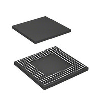
HD6417720BP133BV Renesas Electronics America, HD6417720BP133BV Datasheet - Page 47

HD6417720BP133BV
Manufacturer Part Number
HD6417720BP133BV
Description
SH3-DSP, WITH USB AND LCDC, PB-F
Manufacturer
Renesas Electronics America
Series
SuperH® SH7700r
Datasheet
1.R8A77210C133BAV.pdf
(1478 pages)
Specifications of HD6417720BP133BV
Core Processor
SH-3 DSP
Core Size
32-Bit
Speed
133MHz
Connectivity
FIFO, I²C, IrDA, MMC, SCI, SD, SIO, SIM, USB
Peripherals
DMA, LCD, POR, WDT
Number Of I /o
117
Program Memory Type
ROMless
Ram Size
16K x 8
Voltage - Supply (vcc/vdd)
1.4 V ~ 1.6 V
Data Converters
A/D 4x10b; D/A 2x8b
Oscillator Type
Internal
Operating Temperature
-20°C ~ 75°C
Package / Case
256-BGA
Lead Free Status / RoHS Status
Lead free / RoHS Compliant
Eeprom Size
-
Program Memory Size
-
- Current page: 47 of 1478
- Download datasheet (10Mb)
Figure 38.14 Basic Bus Cycle in Normal Space (External Wait 1 Input) ................................ 1326
Figure 38.15 Basic Bus Cycle in Normal Space
Figure 38.16 CS Extended Bus Cycle in Normal Space
Figure 38.17 Bus Cycle of SRAM with Byte Selection
Figure 38.18 Bus Cycle of SRAM with Byte Selection
Figure 38.19 Read Bus Cycle of Burst ROM
Figure 38.20 Single Read Bus Cycle of SDRAM
Figure 38.21 Single Read Bus Cycle of SDRAM
Figure 38.22 Burst Read Bus Cycle of SDRAM (Single Read × 8)
Figure 38.23 Burst Read Bus Cycle of SDRAM (Single Read × 8)
Figure 38.24 Single Write Bus Cycle of SDRAM
Figure 38.25 Single Write Bus Cycle of SDRAM
Figure 38.26 Burst Write Bus Cycle of SDRAM (Single Write × 8)
Figure 38.27 Burst Write Bus Cycle of SDRAM (Single Write × 8)
Figure 38.28 Burst Read Bus Cycle of SDRAM (Single Read × 8)
Figure 38.29 Burst Read Bus Cycle of SDRAM (Single Read × 8)
Figure 38.30 Burst Read Bus Cycle of SDRAM (Single Read × 8)
Figure 38.31 Burst Write Bus Cycle of SDRAM (Single Write × 8)
R01UH0083EJ0400 Rev. 4.00
Sep 21, 2010
(Software Wait 1, External Wait Valid (WM Bit = 0), No Idle Cycle) .............. 1327
(SW = 1 Cycle, HW = 1 Cycle, External Wait 1 Input)...................................... 1328
(SW = 1 Cycle, HW = 1 Cycle, External Wait 1 Input,
BAS = 0 (UB and LB in Write Cycle Controlled))............................................. 1329
(SW = 1 Cycle, HW = 1 Cycle, External Wait 1 Input,
BAS = 1 (WE in Write Cycle Controlled))......................................................... 1330
(Software Wait 1, External Wait 1 Input, Burst Wait 1, Number of Burst 2) ..... 1331
(Auto Precharge Mode, CAS Latency 2, TRCD = 1 Cycle, TRP = 1 Cycle) ..... 1332
(Auto Precharge Mode, CAS Latency 2, TRCD = 2 Cycles, TRP = 2 Cycles) .. 1333
(Auto Precharge Mode, CAS Latency 2, TRCD = 1 Cycle, TRP = 2 Cycles).... 1334
(Auto Precharge Mode, CAS Latency 2, TRCD = 2 Cycles, TRP = 1 Cycle).... 1335
(Auto Precharge Mode, TRWL = 1 Cycle)......................................................... 1336
(Auto Precharge Mode, TRCD = 3 Cycles, TRWL = 1 Cycle) .......................... 1337
(Auto Precharge Mode, TRCD = 1 Cycle, TRWL = 1 Cycle)............................ 1338
(Auto Precharge Mode, TRCD = 2 Cycles, TRWL = 1 Cycle) .......................... 1339
(Bank Active Mode: ACTV + READ Command, CAS Latency 2,
TRCD = 1 Cycle)................................................................................................ 1340
(Bank Active Mode: READ Command, Same Row Address,
CAS Latency 2, TRCD = 1 Cycle) ..................................................................... 1341
(Bank Active Mode: PRE + ACTV + READ Command,
Different Row Address, CAS Latency 2, TRCD = 1 Cycle) .............................. 1342
(Bank Active Mode: ACTV + WRIT Command, TRCD = 1 Cycle).................. 1343
Page xlvii of lx
Related parts for HD6417720BP133BV
Image
Part Number
Description
Manufacturer
Datasheet
Request
R

Part Number:
Description:
KIT STARTER FOR M16C/29
Manufacturer:
Renesas Electronics America
Datasheet:

Part Number:
Description:
KIT STARTER FOR R8C/2D
Manufacturer:
Renesas Electronics America
Datasheet:

Part Number:
Description:
R0K33062P STARTER KIT
Manufacturer:
Renesas Electronics America
Datasheet:

Part Number:
Description:
KIT STARTER FOR R8C/23 E8A
Manufacturer:
Renesas Electronics America
Datasheet:

Part Number:
Description:
KIT STARTER FOR R8C/25
Manufacturer:
Renesas Electronics America
Datasheet:

Part Number:
Description:
KIT STARTER H8S2456 SHARPE DSPLY
Manufacturer:
Renesas Electronics America
Datasheet:

Part Number:
Description:
KIT STARTER FOR R8C38C
Manufacturer:
Renesas Electronics America
Datasheet:

Part Number:
Description:
KIT STARTER FOR R8C35C
Manufacturer:
Renesas Electronics America
Datasheet:

Part Number:
Description:
KIT STARTER FOR R8CL3AC+LCD APPS
Manufacturer:
Renesas Electronics America
Datasheet:

Part Number:
Description:
KIT STARTER FOR RX610
Manufacturer:
Renesas Electronics America
Datasheet:

Part Number:
Description:
KIT STARTER FOR R32C/118
Manufacturer:
Renesas Electronics America
Datasheet:

Part Number:
Description:
KIT DEV RSK-R8C/26-29
Manufacturer:
Renesas Electronics America
Datasheet:

Part Number:
Description:
KIT STARTER FOR SH7124
Manufacturer:
Renesas Electronics America
Datasheet:

Part Number:
Description:
KIT STARTER FOR H8SX/1622
Manufacturer:
Renesas Electronics America
Datasheet:

Part Number:
Description:
KIT DEV FOR SH7203
Manufacturer:
Renesas Electronics America
Datasheet:


