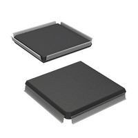
HD6417751RF240V Renesas Electronics America, HD6417751RF240V Datasheet - Page 87

HD6417751RF240V
Manufacturer Part Number
HD6417751RF240V
Description
MPU 1.5/3.3V 0K PB-FREE 256-QFP
Manufacturer
Renesas Electronics America
Series
SuperH® SH7750r
Datasheet
1.D6417751RBP200DV.pdf
(1226 pages)
Specifications of HD6417751RF240V
Core Processor
SH-4
Core Size
32-Bit
Speed
240MHz
Connectivity
EBI/EMI, FIFO, SCI, SmartCard
Peripherals
DMA, POR, WDT
Number Of I /o
39
Program Memory Type
ROMless
Ram Size
48K x 8
Voltage - Supply (vcc/vdd)
1.4 V ~ 1.6 V
Oscillator Type
External
Operating Temperature
-20°C ~ 75°C
Package / Case
256-QFP Exposed Pad, 256-eQFP, 256-HQFP
Lead Free Status / RoHS Status
Lead free / RoHS Compliant
Eeprom Size
-
Program Memory Size
-
Data Converters
-
Available stocks
Company
Part Number
Manufacturer
Quantity
Price
Company:
Part Number:
HD6417751RF240V
Manufacturer:
Renesas Electronics America
Quantity:
10 000
- Current page: 87 of 1226
- Download datasheet (7Mb)
Figure 22.12 Target Write Cycle in Non-Host Mode (Single) .................................................... 954
Figure 22.13 Target Memory Read Cycle in Host Mode (Burst) ................................................ 955
Figure 22.14 Target Memory Write Cycle in Host Mode (Burst) ............................................... 956
Figure 22.15 Master Memory Write Cycle in Host Mode (Burst, With Stepping)...................... 957
Figure 22.16 Target Memory Read Cycle in Host Mode (Burst, With Stepping) ....................... 958
Figure 22.17 Endian Conversion Modes for Peripheral Bus ....................................................... 959
Figure 22.18 Peripheral Bus ↔ PCI Bus Data Alignment .......................................................... 960
Figure 22.19 Endian Control for Local Bus................................................................................. 961
Figure 22.20 Data Alignment at DMA Transfer.......................................................................... 962
Figure 22.21 (1) Data Alignment at Target Memory Transfer (Big-Endian Local Bus) ............ 964
Figure 22.21 (2) Data Alignment at Target Memory Transfer (Little-Endian Local Bus) ......... 965
Figure 22.22 Data Alignment at Target I/O Transfer (Both Big Endian and Little Endian) ....... 966
Figure 22.23 Data Alignment at Target Configuration Transfer
Figure 22.24 Target Bus Timeout Interrupt Generation Example 1
Figure 22.25 Target Bus Timeout Interrupt Generation Example 2 (Example in which
Figure 22.26 Master Bus Timeout Interrupt Generation Example 1 (Example in which
Figure 22.27 Master Bus Timeout Interrupt Generation Example 2 (Example in which
Section 23 Electrical Characteristics
Figure 23.1 EXTAL Clock Input Timing .............................................................................. 1001
Figure 23.2 (1)
Figure 23.2 (2)
Figure 23.3 Power-On Oscillation Settling Time .................................................................. 1002
Figure 23.4 Standby Return Oscillation Settling Time (Return by RESET or MRESET) .... 1002
Figure 23.5 Power-On Oscillation Settling Time .................................................................. 1003
Figure 23.6 Standby Return Oscillation Settling Time (Return by RESET or MRESET) .... 1003
Figure 23.7 Standby Return Oscillation Settling Time (Return by NMI).............................. 1004
Figure 23.8 Standby Return Oscillation Settling Time (Return by IRL3–IRL0)................... 1004
Figure 23.9 PLL Synchronization Settling Time in Case of RESET, MRESET or
Figure 23.10 PLL Synchronization Settling Time in Case of IRL Interrupt............................ 1005
Figure 23.11 Control Signal Timing........................................................................................ 1008
(Both Big Endian and Little Endian)...................................................................... 967
(Example in which the Target Device Asserts STOP at the Sixteenth Clock Cycle
after FRAME Was Asserted).................................................................................. 978
the Target Device Takes 8 Clock Cycles to Prepare for the Third Data Transfer). 979
the Master Device Prepares the Data and Asserts IRDY at the Eighth Clock
Cycle after FRAME Was Asserted) ....................................................................... 979
the Master Device Takes 8 Clock Cycles to Prepare for the Third Data
Transfer following the Second Data Phase) ........................................................... 980
NMI Interrupt ..................................................................................................... 1005
CKIO Clock Output Timing ........................................................................ 1001
CKIO Clock Output Timing ........................................................................ 1001
Rev.4.00 Oct. 10, 2008 Page lxxxv of xcviii
REJ09B0370-0400
Related parts for HD6417751RF240V
Image
Part Number
Description
Manufacturer
Datasheet
Request
R

Part Number:
Description:
KIT STARTER FOR M16C/29
Manufacturer:
Renesas Electronics America
Datasheet:

Part Number:
Description:
KIT STARTER FOR R8C/2D
Manufacturer:
Renesas Electronics America
Datasheet:

Part Number:
Description:
R0K33062P STARTER KIT
Manufacturer:
Renesas Electronics America
Datasheet:

Part Number:
Description:
KIT STARTER FOR R8C/23 E8A
Manufacturer:
Renesas Electronics America
Datasheet:

Part Number:
Description:
KIT STARTER FOR R8C/25
Manufacturer:
Renesas Electronics America
Datasheet:

Part Number:
Description:
KIT STARTER H8S2456 SHARPE DSPLY
Manufacturer:
Renesas Electronics America
Datasheet:

Part Number:
Description:
KIT STARTER FOR R8C38C
Manufacturer:
Renesas Electronics America
Datasheet:

Part Number:
Description:
KIT STARTER FOR R8C35C
Manufacturer:
Renesas Electronics America
Datasheet:

Part Number:
Description:
KIT STARTER FOR R8CL3AC+LCD APPS
Manufacturer:
Renesas Electronics America
Datasheet:

Part Number:
Description:
KIT STARTER FOR RX610
Manufacturer:
Renesas Electronics America
Datasheet:

Part Number:
Description:
KIT STARTER FOR R32C/118
Manufacturer:
Renesas Electronics America
Datasheet:

Part Number:
Description:
KIT DEV RSK-R8C/26-29
Manufacturer:
Renesas Electronics America
Datasheet:

Part Number:
Description:
KIT STARTER FOR SH7124
Manufacturer:
Renesas Electronics America
Datasheet:

Part Number:
Description:
KIT STARTER FOR H8SX/1622
Manufacturer:
Renesas Electronics America
Datasheet:

Part Number:
Description:
KIT DEV FOR SH7203
Manufacturer:
Renesas Electronics America
Datasheet:


